LQ035Q7DB03 Sharp Microelectronics, LQ035Q7DB03 Datasheet - Page 9
LQ035Q7DB03
Manufacturer Part Number
LQ035Q7DB03
Description
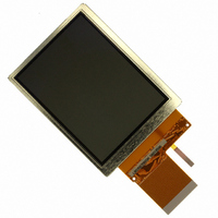
LCD TFT 3.5" 240X320 QVGA
Manufacturer
Sharp Microelectronics
Datasheet
1.LQ035Q7DB03.pdf
(24 pages)
Specifications of LQ035Q7DB03
Display Type
LCD - Color
Display Mode
*
Viewing Area
71.52mm L x 53.64mm W
Dot Pixels
320 x 240 (QVGA)
Lead Free Status / RoHS Status
Contains lead / RoHS non-compliant
Interface
-
Backlight
-
Dot Size
-
Dot Pitch
-
Other names
425-2481
Available stocks
Company
Part Number
Manufacturer
Quantity
Price
Company:

Part Number:
LQ035Q7DB03F
Manufacturer:
SHARP
Quantity:
1 000
Company:
Part Number:
LQ035Q7DB03F
Manufacturer:
LG
Quantity:
1 000


sharp
Supply voltage for source driver
(Analog)
Supply voltage for source driver
(Digital)
Supply voltage
for gate driver
Input voltage for Source driver (Low)
Input voltage for Source driver (High)
Input current for Source driver (Low)
Input current for Source driver (High)
Input voltage for Gate driver (Low)
Input voltage for Gate driver (High)
Input current for Gate driver (Low)
Input current for Gate driver (High)
Common electrode AC component
driving signal
※ Cautions when you turn on or off the power supply
【Note 7-1】DCLK,SPL,SPR,LBR,LP,PS,REV,R0∼R5,G0∼G5 and B0∼B5 terminals are applied.
【Note 7-2】DCLK,SPL,SPR,LBR,LP,REV,R0∼R5,G0∼G5 and B0∼B5 terminals are applied.
【Note 7-3】PS terminal is applied.
【Note 7-4】MOD,CLS,SPS and U/L terminals are applied.
【Note 7-5】VCOMAC should be alternated on VCOMDC every 1 horizontal period and 1 vertical period.
(7)Electrical characteristics
7-1)Recommended operating conditions
B)
【Note 7-6】Calculated reference value(I
LED voltage
LED current
Power consumption
A) TFT-LCD panel driving section
Table 6
① Turn on or off the power supply with simultaneously or the following sequence.
② The input signal of “MOD” Terminals(Pin No.3 and No.4) must be low voltage when turning on
Back light driving section
the power supply, and it is held until more than double vertical periods after VCC is turned on
completely. After then, it must be held high voltage until turning off the power supply.(Connect
Pin No.3 and No.4 terminals to the same signal.)
Parameter
VCOMDC bias is adjusted so as to minimize flicker or maximum contrast every each
module .
Parameter
Turn on … VSHD→VSHA → VEE → VDD
Turn off … VDD → VEE → VSHA→ VSHD
High voltage
Low voltage
DC component
Symbol
W
V
I
L
L
L
VCOMAC
VCOMDC
Symbol
VSHA
VSHD
VIHG
VIHS
VILG
VILS
VDD
I
I
VEE
I
I
I
IHS1
IHS2
IHG
ILS
ILG
MIN
L
−
−
−
×V
Table 5
L
0.8VSHD
0.8VSHD
)
+14.5
GND
GND
-10.5
Min.
+4.5
+3.0
-0.4
-
-
-
-
-
-
0.324
TYP
21.6
15
+15.0
±2.5
-10.0
Typ.
+5.0
+3.3
+0.6
-
-
-
-
-
-
-
-
-
MAX
24
20
−
0.2VSHD
0.2VSHD
VSHD
VSHD
+15.5
Max.
±2.6
1200
+5.5
+1.6
+3.6
-9.5
30
30
4
4
Units
mA
W
V
Unit
Vp-p 【Note 7-5】
μA 【Note 7-1】
μA 【Note 7-2】
μA 【Note 7-3】
μA 【Note 7-4】
μA 【Note 7-4】
V
V
V
V
V
V
V
V
V
Remarks terminal
【Note 7-6】
【Note 7-1】
【Note 7-1】
【Note 7-4】
【Note 7-4】
【Note 7-5】
Ta=25℃
Remarks
LCP-02013−6
GND=0V
Related parts for LQ035Q7DB03
Image
Part Number
Description
Manufacturer
Datasheet
Request
R

Part Number:
Description:
IC FLASH 32MBIT 110NS 56SSOP
Manufacturer:
Sharp Microelectronics
Datasheet:

Part Number:
Description:
IC FLASH 16MBIT 100NS 56TSOP
Manufacturer:
Sharp Microelectronics
Datasheet:

Part Number:
Description:
IC FLASH 64MBIT 120NS 56TSOP
Manufacturer:
Sharp Microelectronics
Datasheet:

Part Number:
Description:
IC FLASH 16MBIT 90NS 48TSOP
Manufacturer:
Sharp Microelectronics
Datasheet:
Part Number:
Description:
IC SRAM 16KBIT 100NS 24DIP
Manufacturer:
Sharp Microelectronics
Datasheet:
Part Number:
Description:
IC SRAM 16KBIT 100NS 24SOP
Manufacturer:
Sharp Microelectronics
Datasheet:
Part Number:
Description:
IC SRAM 64KBIT 100NS 28DIP
Manufacturer:
Sharp Microelectronics
Datasheet:
Part Number:
Description:
IC SRAM 64KBIT 100NS 28SOP
Manufacturer:
Sharp Microelectronics
Datasheet:
Part Number:
Description:
IC SRAM 64KBIT 100NS 28SOP
Manufacturer:
Sharp Microelectronics
Datasheet:
Part Number:
Description:
IC SRAM 256KBIT 70NS 28DIP
Manufacturer:
Sharp Microelectronics
Datasheet:
Part Number:
Description:
IC FLASH 8MBIT 90NS 48TSOP
Manufacturer:
Sharp Microelectronics
Datasheet:
Part Number:
Description:
IC FLASH 8MBIT 85NS 40TSOP
Manufacturer:
Sharp Microelectronics
Datasheet:
Part Number:
Description:
IC FLASH 8MBIT 85NS 40TSOP
Manufacturer:
Sharp Microelectronics
Datasheet:
Part Number:
Description:
IC FLASH 16MBIT 90NS 48TSOP
Manufacturer:
Sharp Microelectronics
Datasheet:
Part Number:
Description:
IC FLASH 16MBIT 70NS 56TSOP
Manufacturer:
Sharp Microelectronics
Datasheet: