HDSP-2533 Avago Technologies US Inc., HDSP-2533 Datasheet
HDSP-2533
Specifications of HDSP-2533


Related parts for HDSP-2533


HDSP-2533 Summary of contents
Page 1
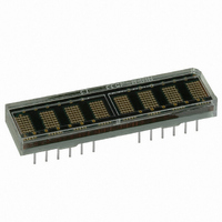
... ESD WARNING: Normal CMOS handling precautions should be observed to avoid static discharge. Features • XY stackable • 128 character ASCII decoder • Programmable functions • 16 user definable characters • Multi-level dimming and blanking • TTL compatible CMOS IC • Wave solderable Applications • Avionics • Computer peripherals • Industrial instrumentation • Medical equipment • Portable data entry devices • Telecommunications • Test equipment Yellow Green HDSP-2531 HDSP-2533 ...
Page 2
... MAX. 4.57 TYP (0.180) PIN #1 IDENTIFIER 2.54 TYP. (0.100) PART NUMBER [4] HDSP-253x X Z YYWW PIN #1 2.54 0.13 10.16 TYP. (0.100 0.005) (0.400) (TOL. NON ACCUM.) Notes: 1. Dimensions are in mm (inches). 2. Unless otherwise specified, tolerance on dimensions is ±0.25 mm (0.010 inch). 3. For yellow and green displays only. 4. Marking is on side opposite pin 1. Absolute Maximum Ratings ...
Page 3
... A 1011 B 1100 C 1101 D 1110 E 1111 F [1] Optical Characteristics at 25° 5 Full Brightness DD LED Color Part Number AlGaAs Red HDSP-2534 High Efficiency Red HDSP-2532 Orange HDSP-2530 Yellow HDSP-2531 Green HDSP-2533 Notes: 1. Refers to the initial case temperature of the device immediately prior to measurement. 2. Dominant wavelength derived from the CIE chromaticity diagram, and represents the single wavelength which defines the color of the device Luminous Intensity Peak Character Average (#) ...
Page 4
Recommended Operating Conditions Parameter Symbol Minimum Supply Voltage V 4.5 DD Electrical Characteristics over Operating Temperature Range 4.5 < V < 5.5 unless otherwise specified DD Parameter Symbol Input Leakage I I (Input without Pull-up) Input Current I IP (Input with Pull-up) I Blank [2,3,4] ...
Page 5
AC Timing Characteristics over Temperature Range V = 4.5 to 5.5 V unless otherwise specified. DD Reference Number Symbol Description 1 t Display Access Time ACC Write Read 2 t Address Setup Time to Chip Enable ACS 3 t Chip Enable Active Time CE Write Read ...
Page 6
Write Cycle Timing Diagram Input Pulse Levels: 0 2.4 V Read Cycle Timing Diagram Input Pulse Levels: 0 2.4 V Output Reference Levels: 0 2.2 V Output Loading = 1 TTL Load and 100 ...
Page 7
Electrical Description Pin Function Description RESET (RST, pin 1) Reset initializes the display. FLASH (FL, pin 2) FL low indicates an access to the Flash RAM and is unaffected by the state of address lines A ADDRESS INPUTS Each location in memory has a distinct address. Address inputs ( pins 3-6, 10) location in the Character RAM, the Flash RAM or a particular row in the UDC (User Defined Character) RAM. A Table 1 shows the logic levels needed to access each section of memory. Table 1. Logic Levels ...
Page 8
8 ...
Page 9
... Display Internal Block Diagram Figure 1 shows the internal block diagram of the HDSP- 253X display. The CMOS IC consists byte Character RAM bit Flash RAM, a 128 character ASCII decoder character UDC RAM, a UDC Address Register, a Control Character RAM Flash RAM User-Defined Character RAM (UDC RAM) User-Defined Character Address Register (UDC Address Register) Control Word Register Character Ram Figure 2 shows the logic levels needed to access the HDSP- 253X Character RAM. During a normal access the CE = “0” ...
Page 10
UDC RAM and UDC Address Register Figure 3 shows the logic levels needed to access the UDC RAM and the UDC Address Register. The UDC Address Register is eight bits wide. The lower four bits (D used to select one of the 16 UDC locations. The upper four bits ( are not used. Once the UDC address has been 4 7 stored in the UDC Address Register, the UDC RAM can be accessed. To completely specify character requires eight write cycles. One cycle is used to store the UDC RAM address in the UDC Address Register. Seven cycles are used to store dot data in the UDC RAM. Data is entered by rows. One ...
Page 11
Control Word Register Figure 6 shows how to access the Control Word Register. This is an eight bit register which performs five functions. They are Brightness control, Flash RAM control, Blinking, Self Test and Clear. Each function is independent of the others. However, all bits are updated during each Control Word write cycle. Brightness (Bits 0-2) Bits 0-2 of the Control Word adjust the brightness of the display. Bits 0-2 are interpreted as a three bit binary code with code (000) corresponding to maximum brightness and code (111) corresponding to a blanked display. In addition to ...
Page 12
... Register are unaffected. All displays which operate with the same clock source must be simultaneously reset to synchronize the Flashing and Blinking functions. Mechanical Considerations The HDSP-253X is assembled by die attaching and wire bonding 280 LED chips and a CMOS thermally con- ductive printed circuit board. A polycarbonate lens placed over the pcb creates an air gap over the LED wire bonds. A backfill epoxy seals the display package. ...
Page 13
... Figure 8. Proper method to manually insert a display. Thermal Considerations The HDSP-253X can operate from -40°C to +85°C. The display’s low thermal resistance allows heat to flow from the CMOS IC to the 24 package pins. Typically, this heat is conducted through the printed circuit board traces to free air. For most applications, no additional heatsinking is needed. Illuminating all 280 LEDs simultaneously at full brightness is not recommended for continuous operation. However, all 280 LEDs can be illuminated simultaneously at full brightness for 10 seconds at 25° ...
Page 14
Table 3 shows the calculated maximum allowable ambient temperature for several different sets of operating condi- tions. The worst case alphanumeric characters (#,@,B) have 20 pixels. Displaying eight 20-pixel characters will not occur in normal operation. Thus, using eight 20-pixel characters to calculate power dissipation will over estimate the power and the IC junction temperature. The average number of pixels per character, supply voltage, brightness level, and number of characters are needed to calculate the power dissipated by the IC. The ambient temperature, power dissipated by the IC, and the thermal resistance ...
Page 15
... Intensity Bin Limits for HDSP-2534 Intensity Range (mcd) Bin Min. I 5.12 J 7.68 K 11.52 L 17.27 M 25.91 Note: Test conditions as specified in Optical Characteristic table. Intensity Bin Limits for HDSP-253x Intensity Range (mcd) Bin Min. G 2.50 H 3.41 I 5.12 J 7.68 K 11.52 Note: Test conditions as specified in Optical Characteristic table. For product information and a complete list of distributors, please go to our web site: Avago, Avago Technologies, and the A logo are trademarks of Avago Technologies in the United States and other countries. Data subject to change. Copyright © ...