HDSP-2533 Avago Technologies US Inc., HDSP-2533 Datasheet - Page 11
HDSP-2533
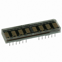
Manufacturer Part Number
HDSP-2533
Description
LED DISPLAY 5X7 8CHAR 5MM GREEN
Manufacturer
Avago Technologies US Inc.
Series
HDSP-253xr
Datasheet
1.HDSP-2533.pdf
(15 pages)
Specifications of HDSP-2533
Display Type
Alphanumeric
Common Pin
*
Package / Case
28-DIP
Color
Green
Size / Dimension
1.69" x .45" (42.9mm x 11.4mm)
Number Of Digits/alpha
8
Digit/alpha Size
0.20" (5mm)
Number Of Digits
8
Character Size
2.54 mm x 4.57 mm
Illumination Color
Green
Wavelength
574 nm
Operating Voltage
5 V
Operating Current
370 mA
Maximum Operating Temperature
+ 85 C
Minimum Operating Temperature
- 40 C
Luminous Intensity
7.5 ucd
Viewing Area (w X H)
40.06 mm x 4.57 mm
Lead Free Status / RoHS Status
Lead free / RoHS Compliant
Lead Free Status / RoHS Status
Lead free / RoHS Compliant, Lead free / RoHS Compliant
Other names
516-1169-5


Control Word Register
Figure 6 shows how to access the Control Word Register.
This is an eight bit register which performs five functions.
They are Brightness control, Flash RAM control, Blinking,
Self Test and Clear. Each function is independent of the
others. However, all bits are updated during each Control
Word write cycle.
Brightness (Bits 0-2)
Bits 0-2 of the Control Word adjust the brightness of the
display. Bits 0-2 are interpreted as a three bit binary code
with code (000) corresponding to maximum brightness
and code (111) corresponding to a blanked display. In
addition to varying the display brightness, bits 0-2 also
vary the average value of I
any brightness level by multiplying the percent bright-
ness level by the value of I
These values of I
Flash Function (Bit 3)
Bit 3 determines whether the flashing character attribute
is on or off. When bit 3 is a “1, ” the output of the Flash RAM
is checked. If the content of a location in the Flash RAM is
a “1, ” the associated digit will flash at approximately 2 Hz.
For an external clock, the blink rate can be calculated by
dividing the clock frequency by 28,672. If the flash enable
bit of the Control Word is a “0, ” the content of the Flash
RAM is ignored. To use this function with multiple display
systems see the Reset section.
Blink Function (Bit 4)
Bit 4 of the Control Word is used to synchronize blinking of
all eight digits of the display. When this bit is a “1” all eight
digits of the display will blink at approximately 2 Hz. The
actual rate is dependent on the clock frequency. For an
external clock, the blink rate can be calculated by dividing
the clock frequency by 28,672. This function will override
the Flash function when it is active. To use this function
with multiple display systems see the Reset section.
Table 2. Current Requirements at Different Brightness Levels for All Colors Except AlGaAs
Symbol
I
11
DD
(V)
DD
D
0
0
0
0
1
1
1
2
are shown in Table 2.
DD
DD
at the 100% brightness level.
. I
DD
D
0
0
1
1
0
0
1
can be calculated at
1
D
0
1
0
1
0
1
0
0
CONTROL SIGNALS
CONTROL WORD ADDRESS
Figure 6. Logic levels to access the control word register.
RST
FL
D
0 NORMAL OPERATION
1 CLEAR FLASH AND CHARACTER RAMS
CONTROL WORD DATA FORMAT
0 = LOGIC 0; 1 = LOGIC 1; X = DO NOT CARE
1
1
C
7
CE
A
D
0
1
0
1
S
4
6
%
Brightness
100
80
53
40
27
20
13
WR
X NORMAL OPERATION; X IS IGNORED
X START SELF TEST; RESULT GIVEN IN X
A
D
0
0
1
1
0
S
3
5
X = 0 FAILED X = 1 PASSED
RD
A
BL
D
0
1
0
1
X
0 DISABLE BLINKING
1 ENABLE BLINKING
2
4
UNDEFINED
WRITE TO DISPLAY
READ FROM DISPLAY
UNDEFINED
A
D
X
F
0 DISABLE FLASH
1 ENABLE FLASH
1
3
V
25°C Typ.
200
160
106
80
54
40
26
DD
A
D
B
X
0
0
0
0
1
1
1
1
0
2
= 5.0 V
D
B
0
0
1
1
0
0
1
1
1
D
B
0
1
0
1
0
1
0
1
0
100%
80%
53%
40%
27%
20%
13%
0%
Units
mA
mA
mA
mA
mA
mA
mA
BRIGHTNESS
CONTROL
LEVELS
Related parts for HDSP-2533
Image
Part Number
Description
Manufacturer
Datasheet
Request
R

Part Number:
Description:
LED 7-SEG 7.6MM CC HE RED RHD
Manufacturer:
Avago Technologies US Inc.
Datasheet:

Part Number:
Description:
LED 7-SEG 7.6MM CA HE RED RHD
Manufacturer:
Avago Technologies US Inc.
Datasheet:

Part Number:
Description:
Seven-Segment Numeric LED Display,2-CHARACTER,Red,DIP
Manufacturer:
Avago Technologies US Inc.
Datasheet:

Part Number:
Description:
Seven-Segment Numeric LED Display,2-CHARACTER,Green,DIP
Manufacturer:
Avago Technologies US Inc.
Datasheet:
Part Number:
Description:
Seven-Segment Numeric LED Display,2-CHARACTER,Green,DIP
Manufacturer:
Avago Technologies US Inc.
Datasheet:
Part Number:
Description:
Seven-Segment Numeric LED Display,2-CHARACTER,Red,DIP
Manufacturer:
Avago Technologies US Inc.
Datasheet:
Part Number:
Description:
Seven-Segment Numeric LED Display,2-CHARACTER,Green,DIP
Manufacturer:
Avago Technologies US Inc.
Datasheet:

Part Number:
Description:
Seven-Segment Numeric LED Display,2-CHARACTER,Orange-Red,DIP
Manufacturer:
Avago Technologies US Inc.
Datasheet:

Part Number:
Description:
LED 7-SEG 14.2MM 2DIG CC HER RHD
Manufacturer:
Avago Technologies US Inc.
Datasheet:

Part Number:
Description:
LED 7-SEG 14.2MM 2DIG CC HER RHD
Manufacturer:
Avago Technologies US Inc.
Datasheet:

Part Number:
Description:
LED 7-SEG 14.2MM 2DIG CA HER RHD
Manufacturer:
Avago Technologies US Inc.
Datasheet:

Part Number:
Description:
LED 7-SEG 14.2MM 2DIG CA GRN RHD
Manufacturer:
Avago Technologies US Inc.
Datasheet:

Part Number:
Description:
LED 7-SEG 14.2MM 2DIG CC GRN RHD
Manufacturer:
Avago Technologies US Inc.
Datasheet:

Part Number:
Description:
LED 7-SEG 14.2MM 2DIG CA GRN RHD
Manufacturer:
Avago Technologies US Inc.
Datasheet:

Part Number:
Description:
LED 7-SEG 14.2MM 2DIG CC GRN RHD
Manufacturer:
Avago Technologies US Inc.
Datasheet: