HDSP-2111 Avago Technologies US Inc., HDSP-2111 Datasheet - Page 14
HDSP-2111
Manufacturer Part Number
HDSP-2111
Description
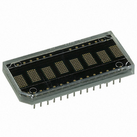
LED DISPLAY 5X7 8CHAR 5MM YLW
Manufacturer
Avago Technologies US Inc.
Series
HDSP-211xr
Datasheet
1.HDSP-2113.pdf
(16 pages)
Specifications of HDSP-2111
Display Type
Alphanumeric
Package / Case
28-DIP
Color
Yellow
Size / Dimension
1.68" L x 0.77" W x 0.21" H (42.59mm x 19.58mm x 5.31mm)
Number Of Digits/alpha
8
Common Pin
*
Digit/alpha Size
0.20" (5mm)
Number Of Digits
8
Character Size
5 mm x 7 mm
Illumination Color
Yellow
Wavelength
583 nm
Operating Voltage
4.5 V to 5.5 V
Maximum Operating Temperature
+ 85 C
Minimum Operating Temperature
- 45 C
Luminous Intensity
7.5 mcd
Lead Free Status / RoHS Status
Lead free / RoHS Compliant
Lead Free Status / RoHS Status
Lead free / RoHS Compliant, Lead free / RoHS Compliant
Other names
516-1162-5
Available stocks
Company
Part Number
Manufacturer
Quantity
Price
Company:

Part Number:
HDSP-2111
Manufacturer:
AVAGO
Quantity:
201
Part Number:
HDSP-2111
Manufacturer:
AGILENT
Quantity:
20 000


Self Test Function (Bits 5, 6)
Bit 6 of the Control Word Regis ter is used to initiate the
self test function. Results of the internal self test are
stored in bit 5 of the Control Word. Bit 5 is a read only bit
where bit 5 = “1” indicates a passed self test and bit 5 =
“0” indicates a failed self test.
Setting bit 6 to a logic 1 will start the self test function.
The built-in self test function of the IC consists of two
internal rou tines which exercise major portions of the
IC and illumin ate all of the LEDs. The first routine cycles
the ASCII decoder ROM through all states and performs
a check sum on the output. If the checksum agrees
with the correct value, bit 5 is set to “1. ” The second
rou tine provides a visual test of the LEDs using the drive
circuitry. This is accomplished by writing checkered and
inverse checkered patterns to the display. Each pattern is
displayed for approxi mately 2 seconds.
During the self test function the display must not be
accessed. The time needed to execute the self test
function is calculated by multiplying the clock period
by 262,144. For example, assume a clock frequency of
58 KHz, then the time to execute the self test function
frequency is equal to (262,144/58,000) = 4.5 second
duration.
At the end of the self test func tion, the Character RAM
is loaded with blanks, the Control Word Register is set to
zeros except for bit 5, the Flash RAM is cleared, and the
UDC Address Register is set to all ones.
Clear Function (Bit 7)
Bit 7 of the Control Word will clear the Character RAM
and the Flash RAM. Setting bit 7 to a “1” will start the
clear func tion. Three clock cycles (110 ms minimum using
the internal refresh clock) are required to complete the
clear function. The display must not be accessed while
the display is being cleared. When the clear function
has been com pleted, bit 7 will be reset to a “0. ” The ASCII
char acter code for a space (20H) will be loaded into the
Character RAM to blank the display and the Flash RAM
will be loaded with “0”s. The UDC RAM, UDC Address
Register, and the re mainder of the Control Word are
unaffected.
Figure 7. Logic levels to reset the display.
14
RST
0
0 = LOGIC 0; 1 = LOGIC 1; X = DO NOT CARE
NOTE:
IF RST, CE, AND WR ARE LOW, UNKNOWN
DATA MAY BE WRITTEN INTO THE DISPLAY.
CE
1
WR
X
RD
X
FL
X
A
4
X
-A
0
D
7
X
-D
0
Display Reset
Figure 7 shows the logic levels needed to Reset the
display. The display should be Reset on Power-up. The
external Reset clears the Character RAM, Flash RAM,
Control Word and resets the internal counters. After the
rising edge of the Reset signal, three clock cycles (110 μs
minimum using the internal refresh clock) are required
to complete the reset sequence. The display must not
be accessed while the display is being reset. The ASCII
Character code for a space (20H) will be loaded into
the Character RAM to blank the display. The Flash RAM
and Control Word Register are loaded with all “0”s. The
UDC RAM and UDC Address Regis ter are unaffected. All
displays which operate with the same clock source must
be simul ta ne ously reset to synchronize the Flashing and
Blinking functions.
Mechanical and Elec trical Considerations
The HDSP-210X/-211X/-250X are 28 pin dual-in-line
packages with 26 external pins. The devices can be
stacked horizontally and verti cally to create arrays of any
size. The HDSP-210X/-211X/-250X are designed to operate
continu ously from -45°C to +85°C with a maxi mum of 20
dots on per character at 5.25 V. Illuminating all thirty-five
dots at full bright ness is not recommended.
The HDSP-210X/-211X/-250X are assembled by die
attaching and wire bonding 280 LED chips and a CMOS
IC to a thermally conductive printed circuit board. A poly-
carbonate lens is placed over the PC board creating an air
gap over the LED wire bonds. A protective cap creates an
air gap over the CMOS IC. Backfill epoxy environment ally
seals the display package. This package construction
makes the display highly tolerant to tem per ature cycling
and allows wave soldering.
The inputs to the IC are pro tected against static discharge
and input current latchup. How ever, for best results
standard CMOS handling precautions should be used.
Prior to use, the HDSP-210X/-211X/-250X should be
stored in antistatic tubes or in conductive material.
During assembly, a grounded conduc tive work area
should be used, and assembly personnel should wear
conductive wrist straps. Lab coats made of synthetic
ma terial should be avoided since they are prone to static
buildup. Input current latchup is caused when the CMOS
inputs are sub jected to either a voltage below ground
(V
V
prevent input current latchup and ESD damage, un used
inputs should be con nected either to ground or to V
Volt ages should not be applied to the inputs until V
has been applied to the display.
DD
IN
) and when a high current is forced into the input. To
< ground) or to a voltage higher than V
DD
(V
IN
DD
DD
>
.
Related parts for HDSP-2111
Image
Part Number
Description
Manufacturer
Datasheet
Request
R

Part Number:
Description:
LED 7-SEG 7.6MM CC HE RED RHD
Manufacturer:
Avago Technologies US Inc.
Datasheet:

Part Number:
Description:
LED 7-SEG 7.6MM CA HE RED RHD
Manufacturer:
Avago Technologies US Inc.
Datasheet:

Part Number:
Description:
Seven-Segment Numeric LED Display,2-CHARACTER,Red,DIP
Manufacturer:
Avago Technologies US Inc.
Datasheet:

Part Number:
Description:
Seven-Segment Numeric LED Display,2-CHARACTER,Green,DIP
Manufacturer:
Avago Technologies US Inc.
Datasheet:
Part Number:
Description:
Seven-Segment Numeric LED Display,2-CHARACTER,Green,DIP
Manufacturer:
Avago Technologies US Inc.
Datasheet:
Part Number:
Description:
Seven-Segment Numeric LED Display,2-CHARACTER,Red,DIP
Manufacturer:
Avago Technologies US Inc.
Datasheet:
Part Number:
Description:
Seven-Segment Numeric LED Display,2-CHARACTER,Green,DIP
Manufacturer:
Avago Technologies US Inc.
Datasheet:

Part Number:
Description:
Seven-Segment Numeric LED Display,2-CHARACTER,Orange-Red,DIP
Manufacturer:
Avago Technologies US Inc.
Datasheet:

Part Number:
Description:
LED 7-SEG 14.2MM 2DIG CC HER RHD
Manufacturer:
Avago Technologies US Inc.
Datasheet:

Part Number:
Description:
LED 7-SEG 14.2MM 2DIG CC HER RHD
Manufacturer:
Avago Technologies US Inc.
Datasheet:

Part Number:
Description:
LED 7-SEG 14.2MM 2DIG CA HER RHD
Manufacturer:
Avago Technologies US Inc.
Datasheet:

Part Number:
Description:
LED 7-SEG 14.2MM 2DIG CA GRN RHD
Manufacturer:
Avago Technologies US Inc.
Datasheet:

Part Number:
Description:
LED 7-SEG 14.2MM 2DIG CC GRN RHD
Manufacturer:
Avago Technologies US Inc.
Datasheet:

Part Number:
Description:
LED 7-SEG 14.2MM 2DIG CA GRN RHD
Manufacturer:
Avago Technologies US Inc.
Datasheet:

Part Number:
Description:
LED 7-SEG 14.2MM 2DIG CC GRN RHD
Manufacturer:
Avago Technologies US Inc.
Datasheet: