HDSP-2111 Avago Technologies US Inc., HDSP-2111 Datasheet - Page 15
HDSP-2111
Manufacturer Part Number
HDSP-2111
Description
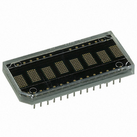
LED DISPLAY 5X7 8CHAR 5MM YLW
Manufacturer
Avago Technologies US Inc.
Series
HDSP-211xr
Datasheet
1.HDSP-2113.pdf
(16 pages)
Specifications of HDSP-2111
Display Type
Alphanumeric
Package / Case
28-DIP
Color
Yellow
Size / Dimension
1.68" L x 0.77" W x 0.21" H (42.59mm x 19.58mm x 5.31mm)
Number Of Digits/alpha
8
Common Pin
*
Digit/alpha Size
0.20" (5mm)
Number Of Digits
8
Character Size
5 mm x 7 mm
Illumination Color
Yellow
Wavelength
583 nm
Operating Voltage
4.5 V to 5.5 V
Maximum Operating Temperature
+ 85 C
Minimum Operating Temperature
- 45 C
Luminous Intensity
7.5 mcd
Lead Free Status / RoHS Status
Lead free / RoHS Compliant
Lead Free Status / RoHS Status
Lead free / RoHS Compliant, Lead free / RoHS Compliant
Other names
516-1162-5
Available stocks
Company
Part Number
Manufacturer
Quantity
Price
Company:

Part Number:
HDSP-2111
Manufacturer:
AVAGO
Quantity:
201
Part Number:
HDSP-2111
Manufacturer:
AGILENT
Quantity:
20 000


Thermal Considerations
The HDSP-210X/-211X/-212X/250X have been designed
to provide a low ther mal resistance path for the CMOS
IC to the 26 package pins. Heat is typically conducted
through the traces of the printed circuit board to free
air. For most applications no addi tional heatsinking is
required.
Measurements were made on a 32 character display
string to determine the thermal resis tance of the display
assembly. Several display boards were con structed using
0.062 in. thick printed circuit material, and one ounce
copper 0.020 in. traces. Some of the device pins were
connected to a heatsink formed by etching a copper
area on the printed circuit board surround ing the display.
A maximally metallized printed circuit board was also
evaluated. The junc tion tem per ature was measured for
displays soldered directly to these PC boards, displays
installed in sockets, and finally displays installed in
sockets with a filter over the display to restrict air flow.
The results of these ther mal resistance measure ments,
Rq
Rq
Ground Connections
Two ground pins are provided to keep the internal IC
logic ground clean. The designer can, when necessary,
route the ana log ground for the LED drivers separately
from the logic ground until an appropriate ground
plane is available. On long inter con nec tions between
the display and the host system, the designer can keep
voltage drops on the analog ground from affect ing the
display logic levels by isolating the two grounds.
The logic ground should be connected to the same
ground poten tial as the logic interface cir cuitry.
The analog ground and the logic ground should be
connected at a common ground which can withstand
the cur rent introduced by the switch ing LED drivers.
When separate ground connec tions are used, the analog
ground can vary from -0.3 V to +0.3 V with re spect to the
logic ground. Volt age below -0.3 V can cause all dots to
be on. Voltage above +0.3 V can cause dimming and dot
mismatch.
Table 3. Thermal Resistance, T
of Heatsinking Material
Heatsinking
Metal
per Device
sq. in.
0
1
3
Max. Metal
4 Board Avg
15
J-A
J-C
.
are shown in Table 3 and include the effects of
W/Sockets
W/O Filter
(Avg.)
31
31
30
29
30
JA
, Using Various Amounts
W/O Sockets
W/O Filter
(Avg.)
30
28
26
25
27
W/Sockets
W/Filter
(Avg.)
35
33
33
32
33
Soldering and Post Solder
Cleaning Instructions for the
HDSP-210X/-211X/-250X
The HDSP-210X/-211X/-250X may be hand soldered or
wave soldered with SN63 solder. When hand soldering,
it is recom mended that an elec tronic ally tempera ture
con trolled and securely grounded soldering iron be used.
For best results, the iron tip temperature should be set at
315°C (600°F). For wave solder ing, a rosin-based RMA flux
can be used. The solder wave tem per a ture should be set
at 245°C ± 5°C (473°F ± 9°F), and the dwell in the wave
should be set between 1
soldering. The preheat tempera ture should not exceed
105°C (221°F) as measured on the solder side of the PC
board.
For addi tional information on solder ing and post solder
clean ing, see Application Note 1027, Soldering LED Com-
ponents.
Contrast Enhancement
The objective of contrast enhance ment is to provide
good readability in a variety of ambient lighting condi-
tions. For informa tion on contrast enhancement see
Appli ca tion Note 1015, Contrast Enhance ment Techniques
for LED Displays.
Units
°C/W
°C/W
°C/W
°C/W
°C/W
1
/
2
to 3 seconds for optimum
Related parts for HDSP-2111
Image
Part Number
Description
Manufacturer
Datasheet
Request
R

Part Number:
Description:
LED 7-SEG 7.6MM CC HE RED RHD
Manufacturer:
Avago Technologies US Inc.
Datasheet:

Part Number:
Description:
LED 7-SEG 7.6MM CA HE RED RHD
Manufacturer:
Avago Technologies US Inc.
Datasheet:

Part Number:
Description:
Seven-Segment Numeric LED Display,2-CHARACTER,Red,DIP
Manufacturer:
Avago Technologies US Inc.
Datasheet:

Part Number:
Description:
Seven-Segment Numeric LED Display,2-CHARACTER,Green,DIP
Manufacturer:
Avago Technologies US Inc.
Datasheet:
Part Number:
Description:
Seven-Segment Numeric LED Display,2-CHARACTER,Green,DIP
Manufacturer:
Avago Technologies US Inc.
Datasheet:
Part Number:
Description:
Seven-Segment Numeric LED Display,2-CHARACTER,Red,DIP
Manufacturer:
Avago Technologies US Inc.
Datasheet:
Part Number:
Description:
Seven-Segment Numeric LED Display,2-CHARACTER,Green,DIP
Manufacturer:
Avago Technologies US Inc.
Datasheet:

Part Number:
Description:
Seven-Segment Numeric LED Display,2-CHARACTER,Orange-Red,DIP
Manufacturer:
Avago Technologies US Inc.
Datasheet:

Part Number:
Description:
LED 7-SEG 14.2MM 2DIG CC HER RHD
Manufacturer:
Avago Technologies US Inc.
Datasheet:

Part Number:
Description:
LED 7-SEG 14.2MM 2DIG CC HER RHD
Manufacturer:
Avago Technologies US Inc.
Datasheet:

Part Number:
Description:
LED 7-SEG 14.2MM 2DIG CA HER RHD
Manufacturer:
Avago Technologies US Inc.
Datasheet:

Part Number:
Description:
LED 7-SEG 14.2MM 2DIG CA GRN RHD
Manufacturer:
Avago Technologies US Inc.
Datasheet:

Part Number:
Description:
LED 7-SEG 14.2MM 2DIG CC GRN RHD
Manufacturer:
Avago Technologies US Inc.
Datasheet:

Part Number:
Description:
LED 7-SEG 14.2MM 2DIG CA GRN RHD
Manufacturer:
Avago Technologies US Inc.
Datasheet:

Part Number:
Description:
LED 7-SEG 14.2MM 2DIG CC GRN RHD
Manufacturer:
Avago Technologies US Inc.
Datasheet: