HDSP-2502 Avago Technologies US Inc., HDSP-2502 Datasheet - Page 11
HDSP-2502
Manufacturer Part Number
HDSP-2502
Description
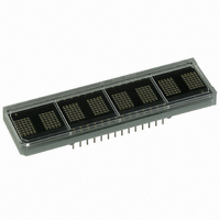
LED DISPLAY 5X7 8CHAR 7MM HE RED
Manufacturer
Avago Technologies US Inc.
Series
HDSP-250xr
Datasheet
1.HDSP-2113.pdf
(16 pages)
Specifications of HDSP-2502
Display Type
Alphanumeric
Package / Case
28-DIP
Color
Red
Size / Dimension
1.68" L x 0.77" W x 0.21" H (42.59mm x 19.58mm x 5.31mm)
Number Of Digits/alpha
8
Common Pin
*
Digit/alpha Size
0.27" (7mm)
Number Of Digits
8
Character Size
5 mm x 7 mm
Illumination Color
Red
Wavelength
635 nm
Operating Voltage
4.5 V to 5.5 V
Maximum Operating Temperature
+ 85 C
Minimum Operating Temperature
- 45 C
Luminous Intensity
7.5 mcd
Lead Free Status / RoHS Status
Lead free / RoHS Compliant
Lead Free Status / RoHS Status
Lead free / RoHS Compliant, Lead free / RoHS Compliant
Other names
516-1164-5
Available stocks
Company
Part Number
Manufacturer
Quantity
Price
Company:

Part Number:
HDSP-2502
Manufacturer:
SEMIKRON
Quantity:
43


Display Internal Block Diagram
Figure 1 shows the internal block diagram of the HDSP-
210X/-211X/-250X displays. The CMOS IC consists of an 8
byte Charac ter RAM, an 8 bit Flash RAM, a 128 character
ASCII decoder, a 16 character UDC RAM, a UDC Address
Character RAM
Flash RAM
User-Defined Character RAM
(UDC RAM)
User-Defined Character
Address Register
(UDC Address Register)
Control Word Register
Character RAM
Figure 2 shows the logic levels needed to access the
HDSP-210X/-211X/-250X Character RAM. During a
normal access, the CE = “0” and either RD = “0” or WR =
“0. ” However, erro neous data may be written into the
Character RAM if the address lines are unstable when CE
= “0” regardless of the logic levels of the RD or WR lines.
Address lines A
Char ac ter RAM. Two types of data can be stored in each
Character RAM location: an ASCII code or a UDC RAM
address. Data bit D
ASCII character and a UDC RAM address. D
the ASCII decoder and D
D
input a UDC address.
11
6
are used to input ASCII data and D
0
-A
2
7
are used to select the location in the
is used to differentiate between the
7
= 1 enables the UDC RAM. D
This RAM stores either ASCII character data or a UDC RAM address.
This is a 1 x 8 RAM which stores Flash data.
This RAM stores the dot pattern for custom characters.
This register is used to provide the address to the UDC RAM when the user is
writing or reading a custom character.
This register allows the user to adjust the display brightness, flash individual
characters, blink, self test, or clear the display.
0
-D
3
7
= 0 enables
are used to
0
-
Register, a Control Word Register, and refresh circuitry
necessary to synchronize the decoding and driving of
eight 5 x 7 dot matrix characters. The major user-acces-
sible portions of the display are listed below:
Figure 2. Logic levels to access the character RAM.
CONTROL SIGNALS
CHARACTER RAM ADDRESS
CHARACTER RAM DATA FORMAT
DISPLAY
0 = LOGIC 0; 1 = LOGIC 1; X = DO NOT CARE
RST
DIG
000
FL
D
1
1
0
1
7
SYMBOL IS ACCESSED IN LOCATION
SPECIFIED BY THE CHARACTER ADDRESS ABOVE
0
DIG
001
CE
A
D
0
1
X
4
6
1
DIG
WR
010
A
D
X
0
0
1
1
1
3
5
2
128 ASCII CODE
DIG
RD
011
A
D
0
1
0
1
X
2
4
CHARACTER
3
ADDRESS
UNDEFINED
WRITE TO DISPLAY
READ FROM DISPLAY
UNDEFINED
DIG
100
A
D
1
3
4
DIG
A
101
D
UDC CODE
0
2
5
DIG
000 = LEFT MOST
111 = RIGHT MOST
110
D
1
6
DIG
111
D
0
7
Related parts for HDSP-2502
Image
Part Number
Description
Manufacturer
Datasheet
Request
R

Part Number:
Description:
LED 7-SEG 7.6MM CC HE RED RHD
Manufacturer:
Avago Technologies US Inc.
Datasheet:

Part Number:
Description:
LED 7-SEG 7.6MM CA HE RED RHD
Manufacturer:
Avago Technologies US Inc.
Datasheet:

Part Number:
Description:
Seven-Segment Numeric LED Display,2-CHARACTER,Red,DIP
Manufacturer:
Avago Technologies US Inc.
Datasheet:

Part Number:
Description:
Seven-Segment Numeric LED Display,2-CHARACTER,Green,DIP
Manufacturer:
Avago Technologies US Inc.
Datasheet:
Part Number:
Description:
Seven-Segment Numeric LED Display,2-CHARACTER,Green,DIP
Manufacturer:
Avago Technologies US Inc.
Datasheet:
Part Number:
Description:
Seven-Segment Numeric LED Display,2-CHARACTER,Red,DIP
Manufacturer:
Avago Technologies US Inc.
Datasheet:
Part Number:
Description:
Seven-Segment Numeric LED Display,2-CHARACTER,Green,DIP
Manufacturer:
Avago Technologies US Inc.
Datasheet:

Part Number:
Description:
Seven-Segment Numeric LED Display,2-CHARACTER,Orange-Red,DIP
Manufacturer:
Avago Technologies US Inc.
Datasheet:

Part Number:
Description:
LED 7-SEG 14.2MM 2DIG CC HER RHD
Manufacturer:
Avago Technologies US Inc.
Datasheet:

Part Number:
Description:
LED 7-SEG 14.2MM 2DIG CC HER RHD
Manufacturer:
Avago Technologies US Inc.
Datasheet:

Part Number:
Description:
LED 7-SEG 14.2MM 2DIG CA HER RHD
Manufacturer:
Avago Technologies US Inc.
Datasheet:

Part Number:
Description:
LED 7-SEG 14.2MM 2DIG CA GRN RHD
Manufacturer:
Avago Technologies US Inc.
Datasheet:

Part Number:
Description:
LED 7-SEG 14.2MM 2DIG CC GRN RHD
Manufacturer:
Avago Technologies US Inc.
Datasheet:

Part Number:
Description:
LED 7-SEG 14.2MM 2DIG CA GRN RHD
Manufacturer:
Avago Technologies US Inc.
Datasheet:

Part Number:
Description:
LED 7-SEG 14.2MM 2DIG CC GRN RHD
Manufacturer:
Avago Technologies US Inc.
Datasheet: