TLMB3100-GS08 Vishay, TLMB3100-GS08 Datasheet

LED PLCC2 BLUE 4.0MCD GAN ON SIC

TLMB3100-GS08

Manufacturer Part Number
TLMB3100-GS08
Description
LED PLCC2 BLUE 4.0MCD GAN ON SIC
Manufacturer
Vishay
Datasheet

Specifications of TLMB3100-GS08

Color
Blue
Millicandela Rating
8mcd
Current - Test
10mA
Wavelength - Dominant
466nm
Wavelength - Peak
428nm
Voltage - Forward (vf) Typ
3.9V
Lens Type
Clear
Lens Style/size
Round, 2.4mm
Package / Case
2-PLCC
Size / Dimension
3.00mm L x 2.80mm W
Height
1.65mm
Viewing Angle
120°
Mounting Type
Surface Mount
Resistance Tolerance
466nm
Led Size
3 mm x 2.8 mm
Illumination Color
Blue
Lens Color/style
Non-Diffused
Wavelength
466 nm
Luminous Intensity
8 mcd
Mounting Style
SMD/SMT
Operating Current
20 mA
Lens Dimensions
2.4 mm
Lens Shape
Flat Round
Maximum Operating Temperature
+ 100 C
Minimum Operating Temperature
- 40 C
Peak Wavelength
428 nm
Lead Free Status / RoHS Status
Lead free / RoHS Compliant
Luminous Flux @ Current - Test
-
Lead Free Status / RoHS Status
Lead free / RoHS Compliant, Lead free / RoHS Compliant
Other names
751-1158-2
SMD LED in PLCC-2 Package
Description
This device has been redesigned in 1998 replacing
SiC by GaN technology to meet the increasing
demand for high efficiency blue LEDs.
The package of the TLMB310. is the PLCC-2 (equiv-
alent to a size B tantalum capacitor).
It consists of a lead frame which is embedded in a
white thermoplast. All LEDs are categorized in lumi-
nous intensity groups. That allows users to assemble
LEDs with uniform appearance.
Features
Parts Table
Absolute Maximum Ratings
T
TLMB310.
Document Number 83034
Rev. 1.7, 31-Aug-04
VISHAY
• GaN on SiC technology
• EIA and ICE standard package
• Compatible with infrared, vapor phase and wave
• Available in 8 mm tape
• Non-diffused lens: excellent for coupling to light
• Luminous intensity ratio in one packaging unit
• ESD class 1
• Lead-free device
TLMB3100
TLMB3101
TLMB3104
TLMB3106
Reverse voltage
DC Forward current
Surge forward current
Power dissipation
Junction temperature
Operating temperature range
amb
solder processes according to CECC
pipes and backlighting
I
Vmax
= 25 °C, unless otherwise specified
/I
Parameter
Vmin
Part
≤ 1.6
T
t
T
Blue, I
Blue, I
Blue, I
Blue, I
p
amb
amb
≤ 10 µs
Color, Luminous Intensity
≤ 60 °C
≤ 60 °C
V
V
V
V
> 4.0 mcd
= (4.0 to 12.5)
= (5.0 to 12.5)
= (5.0 to 20.0)
Test condition
60 °
60 °
60 °
60 °
Applications
Automotive:
Backlighting in dashboards and switches
Telecommunication:
Indicator and backlighting in telephone and fax
Indicator and backlight for audio and video equipment
Indicator and backlight in office equipment
Flat backlight for LCDs, switches and symbols
General use
Angle of Half Intensity (±ϕ)
Symbol
I
T
FSM
V
P
amb
I
T
F
R
V
j
19225
- 40 to + 100
Vishay Semiconductors
Value
100
100
0.1
20
5
GaN on SiC
GaN on SiC
GaN on SiC
GaN on SiC
e3 Pb
TLMB310.
Technology
Pb-free
www.vishay.com
Unit
mW
mA
°C
°C
V
A
1

Related parts for TLMB3100-GS08

TLMB3100-GS08 Summary of contents

Page 1

... Luminous intensity ratio in one packaging unit ≤ 1 Vmax Vmin • ESD class 1 • Lead-free device Parts Table Part Color, Luminous Intensity TLMB3100 Blue, I TLMB3101 Blue, I TLMB3104 Blue, I TLMB3106 Blue, I Absolute Maximum Ratings °C, unless otherwise specified amb TLMB310 ...

Page 2

... T - Ambient Temperature ( ° 10904 amb Figure 1. Power Dissipation vs. Ambient Temperature www.vishay.com 2 Test condition Symbol T stg thJA 2 ) Test condition Part TLMB3100 TLMB3101 TLMB3104 TLMB3106 = 25 °C unless otherwise specified) amb 100 0 15884 Figure 2. Forward Current vs. Ambient Temperature for InGaN VISHAY Value Unit - 100 ° ...

Page 3

... Figure 6. Relative Luminous Flux vs. Forward Current 120 100 350 15849 1000 100 10 0.01 18816 Figure 8. Forward Current vs. Pulse Length TLMB310. Vishay Semiconductors 10 100 I - Forward Current ( 400 450 500 550 600 λ - Wavelenght ( nm ) Figure 7. 0.05 0.1 0.02 0.01 0.2 0.5 ...

Page 4

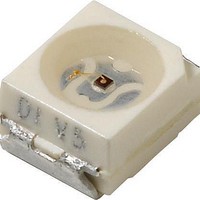
... TLMB310. Vishay Semiconductors Package Dimensions in mm 3.5 ± 0.2 Pin identification C ∅ 2.4 + 0.15 3 Drawing-No. : 6.541-5025.01-4 Issue: 7; 05.04.04 95 11314 www.vishay.com 4 technical drawings according to DIN specifications Mounting Pad Layout A 1.6 (1.9) Dimensions: IR and Vaporphase (Wave Soldering) VISHAY 1.2 area covered with solder resist ...

Page 5

... Various national and international initiatives are pressing for an earlier ban on these substances. Vishay Semiconductor GmbH has been able to use its policy of continuous improvements to eliminate the use of ODSs listed in the following documents. 1. Annex A, B and list of transitional substances of the Montreal Protocol and the London Amendments respectively 2 ...

Page 6

... Information contained herein is intended to provide a product description only. No license, express or implied, by estoppel or otherwise, to any intellectual property rights is granted by this document. Except as provided in Vishay's terms and conditions of sale for such products, Vishay assumes no liability whatsoever, and disclaims any express or implied warranty, relating to sale and/or use of Vishay products including liability or warranties relating to fitness for a particular purpose, merchantability, or infringement of any patent, copyright, or other intellectual property right ...

Related keywords