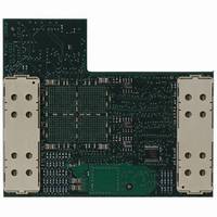
ATICE50POD Atmel, ATICE50POD Datasheet - Page 27

ATICE50POD
Manufacturer Part Number
ATICE50POD
Description
REPLACEMENT POD FOR ICE40,ICE50
Manufacturer
Atmel
Datasheet
1.ATICE50MEM.pdf
(73 pages)
Specifications of ATICE50POD
Accessory Type
POD Replacement Kit
For Use With/related Products
AVR ICE40 and ICE50
Lead Free Status / RoHS Status
Contains lead / RoHS non-compliant
- Current page: 27 of 73
- Download datasheet (2Mb)
ICE50 User Guide
Table 3-3. Data Direction
Notes:
Figure 3-19 shows the timing data for tristating/driving the IO pins. Table 3-4 shows
related typical data.
Figure 3-19. Timing Data
Table 3-4. Timing Data
Notes:
The drive capability of the output buffers are ± 24 mA at 3V V
the driving capability of the actual parts. The operating voltage range of the IO circuits
are 2 V
low voltage (VOLmax) of 1V.
The hysteresis voltage for the input buffers are typically 0.8V at 3V V
V
CC
Delay
t
t
Delay
t
t
t
t
t
t
OHL
OLH
DZH
DHZ
.
DZL
DLZ
IHL
ILH
PORTxy
(3)
(4)
(1)
(2)
(1)
(2)
(3)
(4)
DDRxy
CC
1. tOHL = Time from clearing the PORT register to the output changes
2. tOLH = Time from setting the PORT register to the output changes
3. tIHL = Time from changing the input level to the PIN signal changes (high to low)
4. tILH = Time from changing the input level to the PIN signal changes (low to high)
1. tDZL = time from setting the DDR register to the output is driven low.
2. tDLZ = time from clearing the DDR register to the output is tristated.
3. tDZH = time from setting the DDR register to the output is driven high.
4. tDHZ = time from clearing the DDR register to the output is driven low.
Pxy
to 5.5 V
High Z
CC
Typical Value (2V Target)
Typical Value (2V target)
. At 2V V
t
DZL
13 ns
13 ns
13 ns
13 ns
15 ns
15 ns
15 ns
15 ns
CC
the buffers are able to sink 25 mA with a maximal output
t
DLZ
High Z
t
DZH
Typical Value (5V Target)
Typical Value (5V target)
CC
. This slightly exceeds
10 ns
10 ns
10 ns
10 ns
15 ns
15 ns
15 ns
15 ns
CC
General Description
t
DHZ
and 1.2V at 5.5V
2523A–AVR–11/02
High Z
3-13
Related parts for ATICE50POD
Image
Part Number
Description
Manufacturer
Datasheet
Request
R

Part Number:
Description:
EMULATOR IN CIRCUIT MEGAAVR
Manufacturer:
Atmel
Datasheet:

Part Number:
Description:
DEV KIT FOR AVR/AVR32
Manufacturer:
Atmel
Datasheet:

Part Number:
Description:
INTERVAL AND WIPE/WASH WIPER CONTROL IC WITH DELAY
Manufacturer:
ATMEL Corporation
Datasheet:

Part Number:
Description:
Low-Voltage Voice-Switched IC for Hands-Free Operation
Manufacturer:
ATMEL Corporation
Datasheet:

Part Number:
Description:
MONOLITHIC INTEGRATED FEATUREPHONE CIRCUIT
Manufacturer:
ATMEL Corporation
Datasheet:

Part Number:
Description:
AM-FM Receiver IC U4255BM-M
Manufacturer:
ATMEL Corporation
Datasheet:

Part Number:
Description:
Monolithic Integrated Feature Phone Circuit
Manufacturer:
ATMEL Corporation
Datasheet:

Part Number:
Description:
Multistandard Video-IF and Quasi Parallel Sound Processing
Manufacturer:
ATMEL Corporation
Datasheet:

Part Number:
Description:
High-performance EE PLD
Manufacturer:
ATMEL Corporation
Datasheet:

Part Number:
Description:
8-bit Flash Microcontroller
Manufacturer:
ATMEL Corporation
Datasheet:

Part Number:
Description:
2-Wire Serial EEPROM
Manufacturer:
ATMEL Corporation
Datasheet:


