ATF15XXDK3-SAA100 Atmel, ATF15XXDK3-SAA100 Datasheet - Page 15
ATF15XXDK3-SAA100
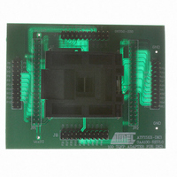
Manufacturer Part Number
ATF15XXDK3-SAA100
Description
ADAPTER SKT ATF15XXB PLCC/TQFP
Manufacturer
Atmel
Datasheet
1.ATF15XXDK3-SAJ44.pdf
(44 pages)
Specifications of ATF15XXDK3-SAA100
Module/board Type
Socket Module - TQFP
For Use With/related Products
ATF15xxDK3
Lead Free Status / RoHS Status
Contains lead / RoHS non-compliant


3605B–PLD–05/06
Hardware Description
2.1.4
2-8
Push-button
Switches with
Selectable Jumpers
for GCLR and OE1
Pins
Table 2-11. Connections of ATF15xx 84-pin PLCC to the Switches for I/O Pins
Table 2-12. Connections of ATF15xx 100-pin TQFP to the Switches for I/O Pins
Atmel CPLD Development/Programmer Board also contains two push-button switches
for the Global Clear (GCLR) and Output Enable (OE1) pins of the CPLD. They allow the
designers to control the logic states of the OE1 and GCLR inputs of the ATF15xx CPLD.
These two switches are labeled SW-GCLR and SW-GOE1 on the Atmel CPLD Develop-
ment/Programmer Board. One end of the SW-GCLR input push-button switch is
connected to ground (GND). The other end of the push-button switch is connected to a
pull-up resistor to VCCIO, and then connected to the GCLR dedicated input pin of the
ATF15xx. It is intended to be used as an active-low reset signal to reset the registers in
the ATF15xx with the JPGCLR selectable jumper set. Similarly, one end of the SW-
GOE1 input push-button switch is connected to ground (GND). The other end of the
push-button switch is connected to a pull-up resistor to VCCIO, and then connected to
the OE1 dedicated input pin of the ATF15xx. It is intended to be used as an active-low
output enable signal to control the enabling/disabling of the tri-state output buffers in the
ATF15xx with the JPGOE selectable jumper set. Figure 2-5 on page 2-9 is the circuit
diagram of these two push-button switches and the jumpers for the GCLR and OE1
pins.
If any of these push-button switches is pressed and the corresponding jumper is set,
then the specific I/O of the CPLD will be driven to a logic low state. Since each push-
button is also connected to a pull-up resistor, the corresponding CPLD input will have a
logic high state if the push-button switch is not pressed with the corresponding select-
able jumper set. If the selectable jumper is not set, the corresponding dedicated input
pin of the CPLD can be considered a “no connect” (NC) pin. Table 2-13 on page 2-9
Push Button #
Push Button #
SW1
SW2
SW3
SW4
SW5
SW6
SW7
SW8
SW1
SW2
SW3
SW4
SW5
SW6
SW7
SW8
ATF15xx-DK3 Development Kit User Guide
PLD Pin #
PLD Pin #
54
51
49
44
80
48
36
44
37
96
98
84
99
9
6
4
Related parts for ATF15XXDK3-SAA100
Image
Part Number
Description
Manufacturer
Datasheet
Request
R

Part Number:
Description:
ADAPTER SKT ATF15XXBE 84/44PLCC
Manufacturer:
Atmel
Datasheet:

Part Number:
Description:
ADAPTER SKT ATF15XXBE 84/84PLCC
Manufacturer:
Atmel
Datasheet:

Part Number:
Description:
KIT DEV 20TSSOP ADAPTER ATF15XX
Manufacturer:
Atmel
Datasheet:

Part Number:
Description:
KIT DEV FOR ATF15XX CPLD'S
Manufacturer:
Atmel
Datasheet:
Part Number:
Description:
ADAPTER FOR ATF15XX-DK2 44TQFP
Manufacturer:
Atmel
Datasheet:
Part Number:
Description:
ADAPTER FOR ATF15XX-DK2 44PLCC
Manufacturer:
Atmel
Datasheet:
Part Number:
Description:
ADAPTER FOR ATF15XX-DK2 68PLCC
Manufacturer:
Atmel
Datasheet:
Part Number:
Description:
ADAPTER FOR ATF15XX-DK2 100TQFP
Manufacturer:
Atmel
Datasheet:

Part Number:
Description:
IC TRANS E-PHEMT 2GHZ SOT-343
Manufacturer:
Avago Technologies US Inc.
Datasheet:
Part Number:
Description:
IC TRANS E-PHEMT 2GHZ SOT-343
Manufacturer:
Avago Technologies US Inc.
Datasheet:

Part Number:
Description:
TRANSISTOR,HEMT,N-CHAN,5.5V V(BR)DSS,175mA I(DSS),SOT-343R
Manufacturer:
Avago Technologies US Inc.
Part Number:
Description:
TRANSISTOR,HEMT,N-CHAN,3V V(BR)DSS,15mA I(DSS),SOT-363
Manufacturer:
Avago Technologies US Inc.
Datasheet:
Part Number:
Description:
TRANSISTOR,HEMT,N-CHAN,4.5V V(BR)DSS,90mA I(DSS),SOT-343R
Manufacturer:
Avago Technologies US Inc.
Datasheet: