ATF15XXDK3-SAA100 Atmel, ATF15XXDK3-SAA100 Datasheet - Page 16
ATF15XXDK3-SAA100
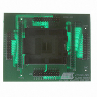
Manufacturer Part Number
ATF15XXDK3-SAA100
Description
ADAPTER SKT ATF15XXB PLCC/TQFP
Manufacturer
Atmel
Datasheet
1.ATF15XXDK3-SAJ44.pdf
(44 pages)
Specifications of ATF15XXDK3-SAA100
Module/board Type
Socket Module - TQFP
For Use With/related Products
ATF15xxDK3
Lead Free Status / RoHS Status
Contains lead / RoHS non-compliant


2.1.5
ATF15xx-DK3 Development Kit User Guide
2 MHz Oscillator and
Clock Selection
Jumper
shows the pin numbers of the GCLR and OE1 dedicated input pins of the ATF15xx in all
the different available package types.
Figure 2-5. Circuit Diagram of Push-button Switches and Selectable Jumpers for
GCLR and OE1
Table 2-13. Pin Numbers of GCLR and OE1
The Clock Selection Jumper, labeled JP-GCLK, on the CPLD Development/Program-
mer Board is a two-position jumper that allows the users to select which GCLK
dedicated input pin (either GCLK1 or GCLK2) of the ATF15xx should be connected to
the output of the 2 MHz oscillator. In addition, the jumper can be removed to allow an
external clock source to be connected to GCLK1 and/or GCLK2 of the ATF15xx. Figure
2-6 is the circuit diagram of the oscillator and selection jumper. Table 2-14 on page 2-10
shows the pin numbers for the GCLK1 and GCLK2 dedicated input pins of the ATF15xx
in all the different available package types.
Note:
Figure 2-6. Circuit Diagram of Oscillator and Clock Selection Jumper
GCLR
OE1
If GCLK1 jumper is set, the jumper will be located toward the side of the board.
On the other hand, if GCLK2 jumper is set, the jumper will be located toward the
middle of the board.
44-pin
TQFP
39
38
44-pin
PLCC
44
1
84-pin
PLCC
84
1
Hardware Description
100-pin
3605B–PLD–05/06
TQFP
89
88
2-9
Related parts for ATF15XXDK3-SAA100
Image
Part Number
Description
Manufacturer
Datasheet
Request
R

Part Number:
Description:
ADAPTER SKT ATF15XXBE 84/44PLCC
Manufacturer:
Atmel
Datasheet:

Part Number:
Description:
ADAPTER SKT ATF15XXBE 84/84PLCC
Manufacturer:
Atmel
Datasheet:

Part Number:
Description:
KIT DEV 20TSSOP ADAPTER ATF15XX
Manufacturer:
Atmel
Datasheet:

Part Number:
Description:
KIT DEV FOR ATF15XX CPLD'S
Manufacturer:
Atmel
Datasheet:
Part Number:
Description:
ADAPTER FOR ATF15XX-DK2 44TQFP
Manufacturer:
Atmel
Datasheet:
Part Number:
Description:
ADAPTER FOR ATF15XX-DK2 44PLCC
Manufacturer:
Atmel
Datasheet:
Part Number:
Description:
ADAPTER FOR ATF15XX-DK2 68PLCC
Manufacturer:
Atmel
Datasheet:
Part Number:
Description:
ADAPTER FOR ATF15XX-DK2 100TQFP
Manufacturer:
Atmel
Datasheet:

Part Number:
Description:
IC TRANS E-PHEMT 2GHZ SOT-343
Manufacturer:
Avago Technologies US Inc.
Datasheet:
Part Number:
Description:
IC TRANS E-PHEMT 2GHZ SOT-343
Manufacturer:
Avago Technologies US Inc.
Datasheet:

Part Number:
Description:
TRANSISTOR,HEMT,N-CHAN,5.5V V(BR)DSS,175mA I(DSS),SOT-343R
Manufacturer:
Avago Technologies US Inc.
Part Number:
Description:
TRANSISTOR,HEMT,N-CHAN,3V V(BR)DSS,15mA I(DSS),SOT-363
Manufacturer:
Avago Technologies US Inc.
Datasheet:
Part Number:
Description:
TRANSISTOR,HEMT,N-CHAN,4.5V V(BR)DSS,90mA I(DSS),SOT-343R
Manufacturer:
Avago Technologies US Inc.
Datasheet: