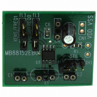
MB88152AEB01-100 Fujitsu Semiconductor America Inc, MB88152AEB01-100 Datasheet

MB88152AEB01-100
Specifications of MB88152AEB01-100
Available stocks
Related parts for MB88152AEB01-100
MB88152AEB01-100 Summary of contents
Page 1
FUJITSU MICROELECTRONICS DATA SHEET Spread Spectrum Clock Generator MB88152A MB88152A-100/101/102/110/111/112 DESCRIPTION MB88152A is a clock generator for EMI (Electro Magnetic Interference) reduction. The peak of unnecessary radiation noise (EMI) can be attenuated by making the oscillation frequency slightly modulate periodically ...
Page 2
MB88152A PRODUCT LINE-UP MB88152A has three kinds of input frequency, and two kinds of modulation type (center/down spread), total six line- ups. Product Input/Output Frequency MB88152A-100 16.6 MHz to 134 MHz MB88152A-101 16.6 MHz to 67 MHz MB88152A-102 40 MHz ...
Page 3
I/O CIRCUIT TYPE Pin Circuit type SEL FREQ FREQ0 FREQ1 XENS CKOUT Note : For XIN and XOUT pins, refer to “ OSCILLATION CIRCUIT”. MB88152A Remarks CMOS hysteresis input • CMOS output = 4 mA • ...
Page 4
MB88152A HANDLING DEVICES Preventing Latch-up A latch-up can occur if, on this device, (a) a voltage higher than V input or output pin or (b) a voltage higher than the rating is applied between V occurs, significantly increases the power ...
Page 5
BLOCK DIAGRAM Modulation rate setting SEL Frequency setting FREQ/FREQ0 Modulation enable / Frequency setting XENS/FREQ1 Reference clock XOUT = 1 MΩ XIN Phase compare Reference 1 clock glitchless IDAC (current output D/A ...
Page 6
MB88152A PIN SETTING When changing the pin setting, the stabilization wait time for the modulation clock is required. The stabilization wait time for the modulation clock takes the maximum value of Lock-Up time in “ ELECTRICAL CHARACTER- ISTICS • AC ...
Page 7
Center spread Spectrum is spread (modulated) by centering on the input frequency. Radiation level Center spread example of ± 1.5% Modulation rate • Down spread Spectrum is spread (modulated) below the input frequency. 3.0% modulation width Radiation level Down ...
Page 8
MB88152A ABSOLUTE MAXIMUM RATINGS Parameter Power supply voltage* Input voltage* Output voltage* Storage temperature Operation junction temperature Output current Overshoot Undershoot * : The parameter is based WARNING: Semiconductor devices can be permanently damaged by application of ...
Page 9
RECOMMENDED OPERATING CONDITIONS Parameter Symbol Power supply voltage V DD FREQ/FREQ0, XENS/FREQ1 “H” level input voltage V IH FREQ/FREQ0, XENS/FREQ1 “L” level input voltage V IL Input clock t DCI duty cycle Operating Ta temperature WARNING: The recommended operating conditions ...
Page 10
MB88152A ELECTRICAL CHARACTERISTICS • DC Characteristics Sym- Parameter bol Power supply current I V Output voltage V Output impedance Z Input capacitance C Load capacitance C 10 (Ta = −40 ° °C, V Pin Conditions 24 MHz ...
Page 11
AC Characteristics Sym- Parameter bol Oscillation frequency f x Input frequency f in Output frequency f OUT Output slew rate SR Output clock duty cycle t DCC Modulation frequency f MOD Number of input clocks ( (n ) MOD ...
Page 12
MB88152A < Definition of modulation frequency and number of input clocks per modulation f (Output frequency) MB88152A contains the modulation period to realize the efficient EMI reduction. The modulation period f depends on the input frequency and changes between f ...
Page 13
OUTPUT CLOCK DUTY CYCLE (t CKOUT = 1/t INPUT FREQUENCY ( XIN OUTPUT SLEW RATE (SR) CKOUT t r Note : SR = (2.4−0. (2.4−0. CYCLE-CYCLE JITTER (t JC ...
Page 14
MB88152A MODULATION WAVEFORM • ±1.5% modulation rate, Example of center spread CKOUT output frequency Frequency at modulation OFF • −1.0% modulation rate, Example of down spread CKOUT output frequency Frequency at modulation OFF 14 + 1.5 % − 1.5 % ...
Page 15
LOCK-UP TIME V DD XIN Setting pin SEL FREQ1/XENS FREQ0/FREQ CKOUT If the setting pin is fixed at the “H” or “L” level, the maximum time after the power is turned on until the set clock signal is output from ...
Page 16
MB88152A OSCILLATION CIRCUIT The left side of figures below shows the connection example about general resonator. The oscillation circuit has the built-in feedback resistance (1 MΩ). The value of capacity (C suitable value of an individual resonator. The right side ...
Page 17
INTERCONNECTION CIRCUIT EXAMPLE SEL Oscillation stabilization capacitance (refer to " OSCILLATION CIRCUIT”.) Capacitor of 10 µF or higher Capacitor about 0.01 µF (connect a capacitor of ...
Page 18
MB88152A EXAMPLE CHARACTERISTICS The condition of the examples of the characteristics is shown as follows : - 20 MHz Use for MB88152A 111 = , Power-supply voltage 3.3 V None load capacity Spectrum analyzer HP4396B is connected with CKOUT. The ...
Page 19
ORDERING INFORMATION Part number MB88152APNF-G-100-JNE1 16.6 MHz to 134 MHz Down spread MB88152APNF-G-101-JNE1 16.6 MHz to 67 MHz Down spread MB88152APNF-G-102-JNE1 40 MHz to 134 MHz MB88152APNF-G-110-JNE1 16.6 MHz to 134 MHz Center spread MB88152APNF-G-111-JNE1 16.6 MHz to 67 MHz ...
Page 20
MB88152A PACKAGE DIMENSION 8-pin plastic SOP (FPT-8P-M02) 8-pin plastic SOP (FPT-8P-M02) +0.25 +.010 1 * 5.05 .199 –0.20 –.008 8 1 1.27(.050) 0.10(.004) 0.10(.004) 2002 FUJITSU LIMITED F08004S-c-4-7 C Please confirm the latest Package dimension by following URL. http://edevice.fujitsu.com/package/en-search/ 20 ...
Page 21
MEMO MB88152A 21 ...
Page 22
MB88152A MEMO 22 ...
Page 23
MEMO MB88152A 23 ...
Page 24
FUJITSU MICROELECTRONICS LIMITED Shinjuku Dai-Ichi Seimei Bldg. 7-1, Nishishinjuku 2-chome, Shinjuku-ku, Tokyo 163-0722, Japan Tel: +81-3-5322-3347 Fax: +81-3-5322-3387 http://jp.fujitsu.com/fml/en/ For further information please contact: North and South America FUJITSU MICROELECTRONICS AMERICA, INC. 1250 E. Arques Avenue, M/S 333 Sunnyvale, CA ...


