EVAL-ADM1178EBZ Analog Devices Inc, EVAL-ADM1178EBZ Datasheet
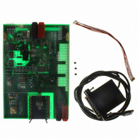
EVAL-ADM1178EBZ
Specifications of EVAL-ADM1178EBZ


Related parts for EVAL-ADM1178EBZ


EVAL-ADM1178EBZ Summary of contents
Page 1
FEATURES Allows safe board insertion and removal from a live backplane Controls supply voltages from 3. 16.5 V Precision current sense amplifier Precision voltage input 12-bit ADC for current and voltage readback Charge-pumped gate drive for external N-channel ...
Page 2
ADM1178 TABLE OF CONTENTS Features .............................................................................................. 1 Applications ....................................................................................... 1 General Description ......................................................................... 1 Functional Block Diagram .............................................................. 1 Revision History ............................................................................... 2 Specifications ..................................................................................... 3 Absolute Maximum Ratings ............................................................ 6 Thermal Characteristics .............................................................. 6 ESD Caution .................................................................................. 6 Pin ...
Page 3
SPECIFICATIONS −40°C to +85°C, typical values Table 1. Parameter VCC PIN Operating Voltage Range Supply Current Undervoltage Lockout, V UVLO Undervoltage Lockout Hysteresis, ...
Page 4
ADM1178 Parameter 1 MONITORING ACCURACY Current Sense Absolute Accuracy 0°C to +70°C 0°C to +85°C −40°C to +85° for ADC Full Scale SENSE Voltage Sense Accuracy 0°C to +70°C 0°C to +85°C −40°C to +85° for ...
Page 5
Parameter Low Period of the SCL Clock High Period of the SCL Clock 4 ADC Conversion Time 5 Fast Overcurrent Response Time Setup Time for a Repeated Start Condition, t SU;STA SDA Output Data Hold Time, t HD;DAT Setup Time ...
Page 6
ADM1178 ABSOLUTE MAXIMUM RATINGS Table 2. Parameter VCC Pin SENSE Pin TIMER Pin ON Pin ALERTB Pin GATE Pin SDA Pin, SCL Pin ADR Pin Storage Temperature Range Operating Temperature Range Lead Temperature Range (Soldering, 10 sec) Junction Temperature Stresses ...
Page 7
PIN CONFIGURATION AND FUNCTION DESCRIPTIONS Table 4. Pin Function Descriptions Pin No. Mnemonic Description 1 VCC Positive Supply Input Pin. The operating supply voltage range is from 3. 16 undervoltage lockout (UVLO) circuit resets the ADM1178 ...
Page 8
ADM1178 TYPICAL PERFORMANCE CHARACTERISTICS 2.0 1.8 1.6 1.4 1.2 1.0 0.8 0.6 0.4 0 (V) CC Figure 4. Supply Current vs. Supply Voltage ...
Page 9
V (V) CC Figure 10. Gate Pull-Down Current vs. Supply Voltage –2 –4 –6 –8 –10 –12 – ...
Page 10
ADM1178 0 –1 –2 –3 –4 –5 – (V) CC Figure 16. Timer Pull-Up Current (Initial Cycle) vs. Supply Voltage 0 –10 –20 –30 –40 –50 –60 –70 – ...
Page 11
V (V) CC Figure 22. Circuit Breaker Limit Voltage vs. Supply Voltage 110 108 V OCFAST 106 104 102 V LIM 100 98 V ...
Page 12
ADM1178 –1 –2 –3 –4 0 500 1000 1500 2000 2500 CODE Figure 28. INL for ADC –1 –2 –3 –4 0 500 1000 1500 2000 2500 CODE Figure 29. ...
Page 13
OVERVIEW OF THE HOT SWAP FUNCTION When circuit boards are inserted into a live backplane, discharged supply bypass capacitors draw large transient currents from the backplane power bus as they charge. Such transient currents can cause permanent damage to connector ...
Page 14
ADM1178 GATE AND TIMER FUNCTIONS DURING A HOT SWAP OPERATION During hot insertion of a board onto a live supply rail at VCC, the abrupt application of supply voltage charges the external FET drain/gate capacitance, which can cause an unwanted ...
Page 15
When the initial timing cycle terminates, the device is ready to start a hot swap operation (assuming that the ON pin is asserted). In the example shown in Figure 33, the ON pin is asserted at the same time as ...
Page 16
ADM1178 VOLTAGE AND CURRENT READBACK In addition to providing hot swap functionality, the ADM1178 contains the components to allow voltage and current readback 2 over bus. The voltage output of the current sense amplifier and the voltage ...
Page 17
SCL SDA ADRA ADRB START BY MASTER FRAME 1 SLAVE ADDRESS 1 SCL (CONTINUED) SDA (CONTINUED) FRAME 3 DATA BYTE 1 SCL SDA ADRA ADRB START BY MASTER ...
Page 18
ADM1178 WRITE AND READ OPERATIONS 2 The I C specification defines several protocols for different types of read and write operations. The operations used in the ADM1178 are discussed in this section. Table 6 shows the abbreviations used in the ...
Page 19
WRITE EXTENDED COMMAND BYTE In the write extended command byte operation, the master device writes to one of the three extended registers of the slave device, as follows: 1. The master device asserts a start condition on SDA. 2. The ...
Page 20
ADM1178 READ VOLTAGE AND/OR CURRENT DATA BYTES Depending on how the device is configured, ADM1191 can be set up to provide information in three ways after a conversion (or conversions): voltage and current readback, voltage only readback, and current only ...
Page 21
Table 15. Status Byte Operations Bit Name Function 0 ADC_OC An ADC-based overcurrent comparison is detected on the last three conversions. 1 ADC_ALERT An ADC-based overcurrent trip has occurred, causing the alert. Cleared by writing to Bit 4 of the ...
Page 22
ADM1178 APPLICATIONS INFORMATION APPLICATIONS WAVEFORMS CH1 1.5A CH2 1.00V M40.0ms CH3 20.0V CH4 10.0V Figure 44. Inrush Current Control into 220 μF Load (Channel Channel Channel 3 = ...
Page 23
ALERTB OUTPUT The ALERTB output is an open-drain pin with 30 V tolerance. This output can be used as an overcurrent flag by connecting it to the general-purpose logic input of a controller. During normal operation, this output is pulled ...
Page 24
... Hot Swap Retry Option 1 ADM1178-1ARMZ-R7 Automatic Retry Version 1 ADM1178-2ARMZ-R7 Latched Off Version 1 EVAL-ADM1178EBZ RoHS Compliant Part. 2 Purchase of licensed I C components of Analog Devices, Inc., or one of its sublicensed Associated Companies conveys a license for the purchaser under the Philips I Patent Rights to use these components system, provided that the system conforms to the I © ...