EVAL-AD9830EBZ Analog Devices Inc, EVAL-AD9830EBZ Datasheet
EVAL-AD9830EBZ
Specifications of EVAL-AD9830EBZ


Related parts for EVAL-AD9830EBZ


EVAL-AD9830EBZ Summary of contents
Page 1
FEATURES +5 V Power Supply 50 MHz Speed On-Chip SINE Look-Up Table On-Chip 10-Bit DAC Parallel Loading Power-Down Option 72 dB SFDR 250 mW Power Consumption 48-Pin TQFP APPLICATIONS DDS Tuning Digital Demodulation MCLK FSELECT FREQ0 REG FREQ1 REG ...
Page 2
AD9830–SPECIFICATIONS Parameter SIGNAL DAC SPECIFICATIONS Resolution Update Rate (f ) MAX I Full Scale OUT Output Compliance DC Accuracy Integral Nonlinearity Differential Nonlinearity 2 DDS SPECIFICATIONS Dynamic Specifications Signal-to-Noise Ratio Total Harmonic Distortion Spurious Free Dynamic Range (SFDR) Narrow Band ...
Page 3
TIMING CHARACTERISTICS Limit MIN MAX Parameter (A Version ...
Page 4
AD9830 ABSOLUTE MAXIMUM RATINGS +25 C unless otherwise noted) A AVDD to AGND . . . . . . . . . . . . . . . . . . . . . . . –0.3 ...
Page 5
Mnemonic Function POWER SUPPLY AVDD Positive power supply for the analog section. A 0.1 F capacitor should be connected between AVDD and AGND. AVDD has a value AGND Analog Ground. DVDD Positive power supply for the digital ...
Page 6
AD9830 TERMINOLOGY Integral Nonlinearity This is the maximum deviation of any code from a straight line passing through the endpoints of the transfer function. The endpoints of the transfer function are zero scale, a point 0.5 LSB below the first ...
Page 7
AVDD = DVDD = + + 200kHz OUT MCLK FREQUENCY – MHz Figure 5. Typical Current Consumption vs. MCLK Frequency –50 AVDD = DVDD ...
Page 8
AD9830 0 –10 –20 –30 –40 –50 –60 –70 –80 –90 START 0Hz RBW 1kHz VBW 3kHz Figure 11 MHz 2.1 MHz, Frequency MCLK OUT Word = ACO8312 0 –10 –20 –30 –40 –50 –60 ...
Page 9
Figure 17. f Word = 547AE148 Register Size Description FREQ0 REG 32 Bits Frequency Register 0. This defines the output frequency, when FSELECT = fraction of the MCLK frequency. FREQ1 REG 32 Bits Frequency Register 1. This ...
Page 10
AD9830 CIRCUIT DESCRIPTION The AD9830 provides an exciting new level of integration for the RF/Communications system designer. The AD9830 combines the Numerical Controlled Oscillator (NCO), SINE Look-Up table, Frequency and Phase Modulators, and a Digital-to-Analog Converter on a single integrated ...
Page 11
Since full-scale current is controlled by R adjustments to R can balance changes made to the load resistor. SET However, if the DAC full-scale output current is significantly ...
Page 12
AD9830 APPLICATIONS The AD9830 contains functions which make it suitable for modulation applications. The part can be used to perform simple modulation such as FSK. More complex modulation schemes such as GMSK and QPSK can also be implemented using the ...
Page 13
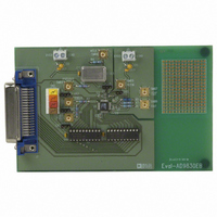
... Prototyping Area An area is available on the evaluation board where the user can add additional circuits to the evaluation test set. Users may want to build custom analog filters for the outputs or add buf- fers and operational amplifiers which are to be used in the final application ...
Page 14
... LK1 PSEL1 11 LK2 PSEL0 10 FSELECT LK3 MCLK 7 MCLK 3 SLEEP DGND DVDD 6,13, 29 36, 39, 41, 46 DVDD LK4 U4 XTAL1 Figure 26. Evaluation Board Layout Links LK5 LK1, LK2, LK3, LK4 Switch SW Sockets SMB1–SMB7 Connectors J2 –14– AVDD 0.1µF C4, C5 AVDD AVDD 10nF 38 ...
Page 15
REV. A OUTLINE DIMENSIONS Dimensions shown in inches and (mm). 48-Lead TQFP (ST-48) 0.063 (1.60) MAX 0.354 (9.00) BSC 0.030 (0.75) 0.057 (1.45) 0.276 (7.0) BSC 0.030 (0.75) 0.053 (1.35) 0.018 (0.45) 0.018 (0.45 SEATING PLANE TOP VIEW ...
Page 16
–16– ...