CDB5467U Cirrus Logic Inc, CDB5467U Datasheet - Page 13
CDB5467U
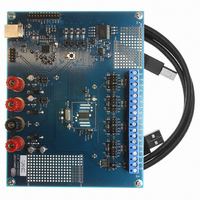
Manufacturer Part Number
CDB5467U
Description
BOARD EVAL FOR CS5467 ADC
Manufacturer
Cirrus Logic Inc
Type
A/Dr
Specifications of CDB5467U
Main Purpose
Power Management, Energy/Power Meter
Embedded
Yes, MCU, 8-Bit
Utilized Ic / Part
CS5467
Primary Attributes
Watt-Hour Meter
Secondary Attributes
Graphical User Interface, SPI™ & USB Interfaces
Product
Data Conversion Development Tools
Maximum Clock Frequency
4 MHz
Interface Type
USB
Supply Voltage (max)
5 V
Supply Voltage (min)
3.3 V
For Use With/related Products
CS5467
Lead Free Status / RoHS Status
Contains lead / RoHS non-compliant
Lead Free Status / RoHS Status
Lead free / RoHS Compliant, Contains lead / RoHS non-compliant
Other names
598-1555
CDB-5467U
CDB-5467U


SWITCHING CHARACTERISTICS
Notes: 19. Pulse output timing is specified at DCLK = 4.096 MHz, E2MODE = 0, and E3MODE[1:0] = 0. Refer to
ABSOLUTE MAXIMUM RATINGS
Notes: 21. VA+ and AGND must satisfy [(VA+) - (AGND)] ≤ + 6.0 V.
DS714F1
WARNING: Operation at or beyond these limits may result in permanent damage to the device.
E1, E2, and E3 Timing
Period
Pulse Width
Rising Edge to Falling Edge
E2 Setup to E1 and/or E3 Falling Edge
E1 Falling Edge to E3 Falling Edge
DC Power Supplies
Input Current, Any Pin Except Supplies
Output Current, Any Pin Except VREFOUT
Power Dissipation
Analog Input Voltage
Digital Input Voltage
Ambient Operating Temperature
Storage Temperature
20. Timing is proportional to the frequency of DCLK.
22. VD+ and AGND must satisfy [(VD+) - (AGND)] ≤ + 6.0 V.
23. Applies to all pins including continuous over-voltage conditions at the analog input pins.
24. Transient current of up to 100 mA will not cause SCR latch-up.
25. Maximum DC input current for a power supply pin is ±50 mA.
26. Total power dissipation, including all input currents and output currents.
6.7 Energy Pulse Outputs
Normal operation is not guaranteed at these extremes
E1
E2
E3
t
4
Parameter
Parameter
t
pw
t
4
t
Figure 2. Timing Diagram for E1, E2, and E3
5
t
period
t
3
on page 20 for more information on pulse output pins.
(Continued)
(Note 19 and 20)
(Notes
(Notes 23, 24, 25)
Positive Analog
All Analog Pins
t
Positive Digital
All Digital Pins
pw
21
(Note 26)
and 22)
t
period
t
3
Symbol
Symbol
V
VD+
I
V
VA+
T
t
OUT
P
T
I
period
INA
IND
IN
stg
.
t
A
D
pw
t
t
t
3
4
5
t
- 0.3
Min
-0.3
-0.3
-0.3
5
-40
-65
Min
500
244
248
1.5
-
-
-
6
Typ
Typ
-
-
-
-
-
-
-
-
-
-
-
-
-
-
(VD+) + 0.3
(VA+) + 0.3
Max
+6.0
+6.0
100
500
150
±10
85
Max
-
-
-
-
-
CS5467
Unit
Unit
mW
mA
mA
°C
°C
µs
µs
µs
µs
µs
V
V
V
V
13
Related parts for CDB5467U
Image
Part Number
Description
Manufacturer
Datasheet
Request
R

Part Number:
Description:
Development Kit
Manufacturer:
Cirrus Logic Inc
Datasheet:
Part Number:
Description:
Development Kit
Manufacturer:
Cirrus Logic Inc
Datasheet:


Part Number:
Description:
High-efficiency PFC + Fluorescent Lamp Driver Reference Design
Manufacturer:
Cirrus Logic Inc
Datasheet:
Part Number:
Description:
Development Kit
Manufacturer:
Cirrus Logic Inc
Datasheet:
Part Number:
Description:
Development Kit
Manufacturer:
Cirrus Logic Inc
Datasheet:

Part Number:
Description:
Development Kit
Manufacturer:
Cirrus Logic Inc
Datasheet:
Part Number:
Description:
Development Kit
Manufacturer:
Cirrus Logic Inc
Datasheet:
Part Number:
Description:
Development Kit
Manufacturer:
Cirrus Logic Inc
Datasheet:
Part Number:
Description:
Development Kit
Manufacturer:
Cirrus Logic Inc
Datasheet:

Part Number:
Description:
EVALUATION BOARD FOR CS8427
Manufacturer:
Cirrus Logic Inc
Datasheet:

Part Number:
Description:
BOARD EVAL FOR CS8416 RCVR
Manufacturer:
Cirrus Logic Inc
Datasheet:

Part Number:
Description:
EVALUATION BOARD FOR CS8420
Manufacturer:
Cirrus Logic Inc
Datasheet:

Part Number:
Description:
KIT DEVELOPMENT EP9315 ARM9
Manufacturer:
Cirrus Logic Inc
Datasheet:

Part Number:
Description:
KIT DEVELOPMENT EP9302 ARM9
Manufacturer:
Cirrus Logic Inc
Datasheet: