CDB5467U Cirrus Logic Inc, CDB5467U Datasheet - Page 14
CDB5467U
Manufacturer Part Number
CDB5467U
Description
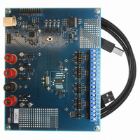
BOARD EVAL FOR CS5467 ADC
Manufacturer
Cirrus Logic Inc
Type
A/Dr
Specifications of CDB5467U
Main Purpose
Power Management, Energy/Power Meter
Embedded
Yes, MCU, 8-Bit
Utilized Ic / Part
CS5467
Primary Attributes
Watt-Hour Meter
Secondary Attributes
Graphical User Interface, SPI™ & USB Interfaces
Product
Data Conversion Development Tools
Maximum Clock Frequency
4 MHz
Interface Type
USB
Supply Voltage (max)
5 V
Supply Voltage (min)
3.3 V
For Use With/related Products
CS5467
Lead Free Status / RoHS Status
Contains lead / RoHS non-compliant
Lead Free Status / RoHS Status
Lead free / RoHS Compliant, Contains lead / RoHS non-compliant
Other names
598-1555
CDB-5467U
CDB-5467U


4. SIGNAL PATH DESCRIPTION
The data flow for voltage and current measurement and
the other calculations are shown in Figures 3, 4, and 5.
4.1 Analog-to-Digital Converters
Voltage1 channel and voltage2/temperature channel
use second-order delta-sigma modulators and the two
current channels use fourth-order delta-sigma modula-
tors to convert the analog inputs to single-bit digital data
streams. The converters sample at a rate of DCLK/8.
This high sampling provides a wide dynamic range and
simplifies anti-alias filter design.
4.2 Decimation Filters
The single-bit modulator output data is widened to 24
bits and down-sampled to DCLK/1024 with low-pass
decimation filters. These decimation filters are third-or-
der Sinc. Their outputs are passed through third-order
14
FGA
FGA
1
2
2
Figure 3. Signal Flow for V1, I1, P1, Q1 Measurements
Figure 4. Signal Flow for V2, I2, P2, Q2 Measurements
Control Register
V1
V2
I1
I2
VHPF1 IHPF1
OFF
OFF
VHPF2 IHPF2
OFF
OFF
IIR “anti-sinc” filters, used to compensate for the ampli-
tude roll-off of the decimation filters.
4.3 Phase Compensation
Phase compensation changes the phase of current rel-
ative to voltage by changing the sampling time in the
decimation filters. The amount of phase shift is set by
bits PC[7:0] in the Configuration register ( Config ) for
channel 1 and bits PC[7:0] in the Control register ( Ctrl )
for channel 2.
Phase compensation, PC[7:0] is a signed two’s comple-
ment binary value in the range of -1.0 to almost +1.0
output word rate (OWR) samples. For a sample rate of
4000 Hz, the delay range is ±250 uS, a phase shift of
±4.5° at 50 Hz and ±5.4° at 60 Hz. The step size would
be 0.0352° at 50 Hz and 0.0422° at 60 Hz at this sample
rate.
V1
V2
I1
I2
GAIN
GAIN
GAIN
GAIN
V2
I2
P2
CS5467
DS714F1
V2Q
Q2
Related parts for CDB5467U
Image
Part Number
Description
Manufacturer
Datasheet
Request
R

Part Number:
Description:
Development Kit
Manufacturer:
Cirrus Logic Inc
Datasheet:
Part Number:
Description:
Development Kit
Manufacturer:
Cirrus Logic Inc
Datasheet:


Part Number:
Description:
High-efficiency PFC + Fluorescent Lamp Driver Reference Design
Manufacturer:
Cirrus Logic Inc
Datasheet:
Part Number:
Description:
Development Kit
Manufacturer:
Cirrus Logic Inc
Datasheet:
Part Number:
Description:
Development Kit
Manufacturer:
Cirrus Logic Inc
Datasheet:

Part Number:
Description:
Development Kit
Manufacturer:
Cirrus Logic Inc
Datasheet:
Part Number:
Description:
Development Kit
Manufacturer:
Cirrus Logic Inc
Datasheet:
Part Number:
Description:
Development Kit
Manufacturer:
Cirrus Logic Inc
Datasheet:
Part Number:
Description:
Development Kit
Manufacturer:
Cirrus Logic Inc
Datasheet:

Part Number:
Description:
EVALUATION BOARD FOR CS8427
Manufacturer:
Cirrus Logic Inc
Datasheet:

Part Number:
Description:
BOARD EVAL FOR CS8416 RCVR
Manufacturer:
Cirrus Logic Inc
Datasheet:

Part Number:
Description:
EVALUATION BOARD FOR CS8420
Manufacturer:
Cirrus Logic Inc
Datasheet:

Part Number:
Description:
KIT DEVELOPMENT EP9315 ARM9
Manufacturer:
Cirrus Logic Inc
Datasheet:

Part Number:
Description:
KIT DEVELOPMENT EP9302 ARM9
Manufacturer:
Cirrus Logic Inc
Datasheet: