CDB5467U Cirrus Logic Inc, CDB5467U Datasheet - Page 18
CDB5467U
Manufacturer Part Number
CDB5467U
Description
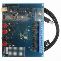
BOARD EVAL FOR CS5467 ADC
Manufacturer
Cirrus Logic Inc
Type
A/Dr
Specifications of CDB5467U
Main Purpose
Power Management, Energy/Power Meter
Embedded
Yes, MCU, 8-Bit
Utilized Ic / Part
CS5467
Primary Attributes
Watt-Hour Meter
Secondary Attributes
Graphical User Interface, SPI™ & USB Interfaces
Product
Data Conversion Development Tools
Maximum Clock Frequency
4 MHz
Interface Type
USB
Supply Voltage (max)
5 V
Supply Voltage (min)
3.3 V
For Use With/related Products
CS5467
Lead Free Status / RoHS Status
Contains lead / RoHS non-compliant
Lead Free Status / RoHS Status
Lead free / RoHS Compliant, Contains lead / RoHS non-compliant
Other names
598-1555
CDB-5467U
CDB-5467U


5. PIN DESCRIPTIONS
5.1 Analog Pins
The CS5467 has four differential inputs: VIN1 ±, VIN2 ±,
IIN1 ± , and IIN2 ± are the voltage1, voltage2, current1,
and current2 inputs, respectively. A single-ended power
fail monitor input, voltage reference input, and voltage
reference output are also available.
5.1.1 Voltage1 & Voltage2 Inputs
The output of the line voltage resistive divider or trans-
former is connected to the VIN1+ (VIN2+) and VIN1-
(VIN2-) input pins of the CS5467. The voltage channel
is equipped with a 10x, fixed-gain amplifier. The
full-scale signal level that can be applied to the voltage
channel is ±250 mV. If the input signal is a sine wave,
the
250 mVp /
ly 70.7% of maximum peak voltage.
5.1.2 Current1 & Current2 Inputs
The output of the current-sensing resistor or transform-
er is connected to the IIN1+ (IIN2+) and IIN1- (IIN2-) in-
put pins of the CS5467. To accommodate different
current-sensing elements, the current channel incorpo-
rates a programmable gain amplifier (PGA) with two se-
lectable input gains. The full-scale signal level for the
current channels is ±50 mV or ±250 mV. If the input sig-
nal is a sine wave, the maximum RMS voltage is
35.35 mVRMS or 176.78 mVRMS which is approxi-
mately 70.7% of maximum peak voltage.
5.1.3 Power Fail Monitor Input
An analog input (PFMON) is provided to determine
when a power loss is imminent. By connecting a resis-
tive divider from the unregulated meter power supply to
the PFMON input, an interrupt can be generated, or the
Low Supply Detected (LSD) Status register bit can be
monitored to indicate low-supply conditions. The
PFMON input has a comparator that trips around the
level of the voltage reference input (VREFIN).
5.1.4 Voltage Reference Input
The CS5467 requires a stable voltage reference of
2.5 V applied to the VREFIN pin. This reference can be
supplied from an external voltage reference or from the
VREFOUT output. A bypass capacitor of at least 0.1 µ F
is recommended at the VREFIN pin.
5.1.5 Voltage Reference Output
The CS5467 generates a 2.5 V reference (VREFOUT).
It is suitable for driving the VREFIN pin, but has very lit-
tle fan-out capacity and is not recommended for driving
external circuits.
18
maximum
√
2
≈
176.78 mVRMS which is approximate-
RMS
voltage
is
5.1.6 Crystal Oscillator
An external quartz crystal can be connected to the XIN
and XOUT pins as shown in Figure 7. To reduce system
cost, each pin is supplied with an on-chip, phase-shift-
ing capacitor to ground.
.
Alternatively, an external clock source can be connect-
ed to the XIN pin.
5.2 Digital Pins
5.2.1 Reset Input
The active-low RESET pin, when asserted, will halt all
CS5467 operations and reset internal hardware regis-
ters and states. When de-asserted, an initialization se-
quence begins, setting default register values.
5.2.2 CPU Clock Output
A logic-level clock output (CPUCLK) is provided at the
crystal frequency to drive an external CPU or microcon-
troller clock. Two phase choices are available.
5.2.3 Interrupt Output
The INT pin indicates an enabled Internal Status regis-
ter ( Status ) bit is set. Status register bits indicate condi-
tions such as data ready, modulator oscillations, low
supply, voltage sag, current faults, numerical overflows,
and result updates.
5.2.4 Energy Pulse Outputs
The CS5467 provides three pins (E1, E2, E3) for pulse
energy outputs. These pins can also be used to output
other conditions, such as voltage1 sign, power fail mon-
itor, or energy sign.
Figure 7. Oscillator Connections
DGND
XOUT
XIN
C1
C2
C1 =
C2 =
Oscillator
22 pF
Circuit
CS5467
DS714F1
Related parts for CDB5467U
Image
Part Number
Description
Manufacturer
Datasheet
Request
R

Part Number:
Description:
Development Kit
Manufacturer:
Cirrus Logic Inc
Datasheet:
Part Number:
Description:
Development Kit
Manufacturer:
Cirrus Logic Inc
Datasheet:


Part Number:
Description:
High-efficiency PFC + Fluorescent Lamp Driver Reference Design
Manufacturer:
Cirrus Logic Inc
Datasheet:
Part Number:
Description:
Development Kit
Manufacturer:
Cirrus Logic Inc
Datasheet:
Part Number:
Description:
Development Kit
Manufacturer:
Cirrus Logic Inc
Datasheet:

Part Number:
Description:
Development Kit
Manufacturer:
Cirrus Logic Inc
Datasheet:
Part Number:
Description:
Development Kit
Manufacturer:
Cirrus Logic Inc
Datasheet:
Part Number:
Description:
Development Kit
Manufacturer:
Cirrus Logic Inc
Datasheet:
Part Number:
Description:
Development Kit
Manufacturer:
Cirrus Logic Inc
Datasheet:

Part Number:
Description:
EVALUATION BOARD FOR CS8427
Manufacturer:
Cirrus Logic Inc
Datasheet:

Part Number:
Description:
BOARD EVAL FOR CS8416 RCVR
Manufacturer:
Cirrus Logic Inc
Datasheet:

Part Number:
Description:
EVALUATION BOARD FOR CS8420
Manufacturer:
Cirrus Logic Inc
Datasheet:

Part Number:
Description:
KIT DEVELOPMENT EP9315 ARM9
Manufacturer:
Cirrus Logic Inc
Datasheet:

Part Number:
Description:
KIT DEVELOPMENT EP9302 ARM9
Manufacturer:
Cirrus Logic Inc
Datasheet: