CDB5467U Cirrus Logic Inc, CDB5467U Datasheet - Page 21
CDB5467U
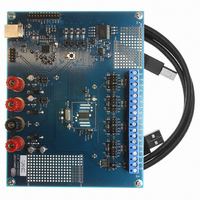
Manufacturer Part Number
CDB5467U
Description
BOARD EVAL FOR CS5467 ADC
Manufacturer
Cirrus Logic Inc
Type
A/Dr
Specifications of CDB5467U
Main Purpose
Power Management, Energy/Power Meter
Embedded
Yes, MCU, 8-Bit
Utilized Ic / Part
CS5467
Primary Attributes
Watt-Hour Meter
Secondary Attributes
Graphical User Interface, SPI™ & USB Interfaces
Product
Data Conversion Development Tools
Maximum Clock Frequency
4 MHz
Interface Type
USB
Supply Voltage (max)
5 V
Supply Voltage (min)
3.3 V
For Use With/related Products
CS5467
Lead Free Status / RoHS Status
Contains lead / RoHS non-compliant
Lead Free Status / RoHS Status
Lead free / RoHS Compliant, Contains lead / RoHS non-compliant
Other names
598-1555
CDB-5467U
CDB-5467U


E3MODE[1:0] in the Modes register when E1MODE is
When both E2MODE bits are high, the E1MODE bits
are enabled, allowing active, apparent, reactive, or wide
band reactive energy for both energy channels to be
output on E1 and E2. Table 6 lists the functions of E1
and E2 with E1MODE enabled.
When E1MODE bits are enabled, the E3 pin outputs ei-
ther the power fail monitor status, or the sign of the E1
and E2 outputs. Table 7 list the functions of the E3 pin
using E3MODE[1:0] in the Modes register when
E1MODE is enabled .
DS714F1
not enabled.
E3MODE1 E3MODE0
E1MODE1 E1MODE0
E3MODE1 E3MODE0
0
0
1
1
0
0
1
1
0
0
1
1
Table 7. E3 Pin with E1MODE enabled
Table 5. E3 Pin Configuration
Table 6. E1 / E2 Modes
0
1
0
1
0
1
0
1
0
1
0
1
Total Apparent Energy
Total Reactive Energy
Wideband Reactive
Power Fail Monitor
Power Fail Monitor
Apparent Energy
Reactive Energy
E1 / E2 outputs
Voltage1 Sign
Active Energy
Energy Sign
E3 output
E3 output
not used
not used
6.8 No Load Threshold
The No Load Threshold register ( Load
zero out the contents of E
their magnitude is less than the Load
6.9 Energy Pulse Width
Note: Energy Pulse Width ( PulseWidth ) only applies to
E1, E2, or E3 pins that are configured to output pulses.
When any are configured to output steady-state signals,
such as voltage1 sign, power fail monitor, or energy
sign, pulse widths and output rates do not apply.
The pulse width time (t
in the PulseWidth register which is an integer multiple of
the sample or output word rate (OWR). At OWR of
4000 Hz (a period of 250 uS) t
250 uS. By default, PulseWidth is set to 1.
6.10 Energy Pulse Rate
The full-scale pulse frequency of enabled E1, E2, E3
pins is the value in PulseRate x output word rate
(OWR)/2. The actual pulse frequency is the full-scale
pulse frequency multiplied by the pulse register’s
( E
Example:
If the output word rate (OWR) is 4000 Hz, and the
PulseRate register is set to 0.05, the full-rate pulse fre-
quency is 0.05 x 4000 / 2 = 100 Hz. If the E
ter, driving E1, is 0.4567, the pulse output rate on E1 will
be 100 Hz x 0.4567 = 45.67 Hz.
6.11 Voltage Sag/Current Fault Detection
Voltage sag detection is used to determine when aver-
aged voltage falls below a predetermined level for a
specified interval of time. Current fault detection deter-
mines when averaged current falls below a predeter-
mined level for a specified interval of time.
The specified interval of time (duration) is set by the val-
ue in the V1Sag
( I2Fault
fault) disables the detect feature for the given channel.
The value is in output word rate (OWR) samples. The
predetermined level is set by the values in the
V1Sag
( I2Fault
PULSE
LEVEL
LEVEL
DUR
, S
PULSE
) registers. Setting any of these to zero (de-
) registers.
( V2Sag
, or Q
DUR
pw
PULSE
LEVEL
) in
( V2Sag
PULSE
Figure
) value.
)
and Q
DUR
pw
and
2, is set by the value
) and I1Fault
MIN
PULSE
= PulseWidth x
MIN
register value.
CS5467
PULSE
I1Fault
) is used to
registers if
regis-
LEVEL
DUR
21
Related parts for CDB5467U
Image
Part Number
Description
Manufacturer
Datasheet
Request
R

Part Number:
Description:
Development Kit
Manufacturer:
Cirrus Logic Inc
Datasheet:
Part Number:
Description:
Development Kit
Manufacturer:
Cirrus Logic Inc
Datasheet:


Part Number:
Description:
High-efficiency PFC + Fluorescent Lamp Driver Reference Design
Manufacturer:
Cirrus Logic Inc
Datasheet:
Part Number:
Description:
Development Kit
Manufacturer:
Cirrus Logic Inc
Datasheet:
Part Number:
Description:
Development Kit
Manufacturer:
Cirrus Logic Inc
Datasheet:

Part Number:
Description:
Development Kit
Manufacturer:
Cirrus Logic Inc
Datasheet:
Part Number:
Description:
Development Kit
Manufacturer:
Cirrus Logic Inc
Datasheet:
Part Number:
Description:
Development Kit
Manufacturer:
Cirrus Logic Inc
Datasheet:
Part Number:
Description:
Development Kit
Manufacturer:
Cirrus Logic Inc
Datasheet:

Part Number:
Description:
EVALUATION BOARD FOR CS8427
Manufacturer:
Cirrus Logic Inc
Datasheet:

Part Number:
Description:
BOARD EVAL FOR CS8416 RCVR
Manufacturer:
Cirrus Logic Inc
Datasheet:

Part Number:
Description:
EVALUATION BOARD FOR CS8420
Manufacturer:
Cirrus Logic Inc
Datasheet:

Part Number:
Description:
KIT DEVELOPMENT EP9315 ARM9
Manufacturer:
Cirrus Logic Inc
Datasheet:

Part Number:
Description:
KIT DEVELOPMENT EP9302 ARM9
Manufacturer:
Cirrus Logic Inc
Datasheet: