CDB5467U Cirrus Logic Inc, CDB5467U Datasheet - Page 40
CDB5467U
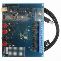
Manufacturer Part Number
CDB5467U
Description
BOARD EVAL FOR CS5467 ADC
Manufacturer
Cirrus Logic Inc
Type
A/Dr
Specifications of CDB5467U
Main Purpose
Power Management, Energy/Power Meter
Embedded
Yes, MCU, 8-Bit
Utilized Ic / Part
CS5467
Primary Attributes
Watt-Hour Meter
Secondary Attributes
Graphical User Interface, SPI™ & USB Interfaces
Product
Data Conversion Development Tools
Maximum Clock Frequency
4 MHz
Interface Type
USB
Supply Voltage (max)
5 V
Supply Voltage (min)
3.3 V
For Use With/related Products
CS5467
Lead Free Status / RoHS Status
Contains lead / RoHS non-compliant
Lead Free Status / RoHS Status
Lead free / RoHS Compliant, Contains lead / RoHS non-compliant
Other names
598-1555
CDB-5467U
CDB-5467U


9. SYSTEM CALIBRATION
9.1 Calibration
The CS5467 provides DC offset and gain calibration
that can be applied to the voltage and current measure-
ments, and AC offset calibration which can be applied to
the voltage and current RMS calculations.
Since the voltage and current channels have indepen-
dent offset and gain registers, offset and gain calibra-
tion can be performed on any channel independently.
The data flow of the calibration is shown in
The CS5467 must be operating in its active state and
ready to accept valid commands. Refer to
mands
The value in the Cycle Count register ( N ) determines
the number of output word rate (OWR) samples that are
averaged during a calibration. DC offset and gain cali-
brations take at least N + T
calibrations take at least 6( N ) + T
is increased, the accuracy of calibration results tends to
also increase.
The DRDY bit in the Status register will be set at the
completion of Calibration commands. If an overflow oc-
curs during calibration, other Status register bits may be
set as well.
9.1.1 Offset Calibration
During offset calibrations, no line voltage or current
should be applied to the meter. A zero-volt differential
signal can also be applied to the voltage inputs VIN1 ±
( VIN2 ±) or current inputs IIN1 ± (IIN2 ±) of the CS5467.
(see
40
Figure
In
on page 25.
11.)
Modulator
= READABLE/WRITABLE REGISTERS.
Filter
DC Offset
SETTLE
I1
I2
DCOFF
DCOFF
Negate
SETTLE
, V1
, V2
+
samples. AC offset
AC Gain
DCOFF
DCOFF
Figure 10. Calibration Data Flow
,
samples. As N
I1
I2
Figure
GAIN
GAIN
7.6 Com-
, V1
, V2
X
DC
1
GAIN
GAIN
AVG
DC Gain
10.
,
Σ
÷
V1, I1, V2, I2
N
N
9.1.1.1 DC Offset Calibration
The DC Offset Calibration command measures and av-
erages DC values read on specified voltage or current
channels at zero input and stores the inverse result in
the associated offset registers. This will be added to in-
stantaneous measurements in subsequent conver-
sions, removing the offset.
Gain registers for channels being calibrated should be
set to 1.0 prior to performing DC offset calibration.
9.1.1.2 AC Offset Calibration
The AC Offset Calibration command measures the re-
sidual RMS values read on specified voltage or current
channels at zero input and stores the inverse result in
the associated AC offset registers. This will be added to
RMS measurements in subsequent conversions, re-
moving the offset.
AC offset registers for channels being calibrated should
first be cleared prior to performing the calibration.
DC AVG
X
CM + -
0V + -
External
Connections
Figure 11. System Calibration of Offset
AIN+
AIN-
Σ
N
RMS
0.6
÷
N
+
-
√
AC Offset
XGAIN
I1
I2
ACOFF
ACOFF
+
Negate
, V1
, V2
+
+
ACOFF
ACOFF
RMS
,
I1
CS5467
I2
RMS
RMS
DS714F1
, V1
, V2
+
-
RMS
RMS
,
Related parts for CDB5467U
Image
Part Number
Description
Manufacturer
Datasheet
Request
R

Part Number:
Description:
Development Kit
Manufacturer:
Cirrus Logic Inc
Datasheet:
Part Number:
Description:
Development Kit
Manufacturer:
Cirrus Logic Inc
Datasheet:


Part Number:
Description:
High-efficiency PFC + Fluorescent Lamp Driver Reference Design
Manufacturer:
Cirrus Logic Inc
Datasheet:
Part Number:
Description:
Development Kit
Manufacturer:
Cirrus Logic Inc
Datasheet:
Part Number:
Description:
Development Kit
Manufacturer:
Cirrus Logic Inc
Datasheet:

Part Number:
Description:
Development Kit
Manufacturer:
Cirrus Logic Inc
Datasheet:
Part Number:
Description:
Development Kit
Manufacturer:
Cirrus Logic Inc
Datasheet:
Part Number:
Description:
Development Kit
Manufacturer:
Cirrus Logic Inc
Datasheet:
Part Number:
Description:
Development Kit
Manufacturer:
Cirrus Logic Inc
Datasheet:

Part Number:
Description:
EVALUATION BOARD FOR CS8427
Manufacturer:
Cirrus Logic Inc
Datasheet:

Part Number:
Description:
BOARD EVAL FOR CS8416 RCVR
Manufacturer:
Cirrus Logic Inc
Datasheet:

Part Number:
Description:
EVALUATION BOARD FOR CS8420
Manufacturer:
Cirrus Logic Inc
Datasheet:

Part Number:
Description:
KIT DEVELOPMENT EP9315 ARM9
Manufacturer:
Cirrus Logic Inc
Datasheet:

Part Number:
Description:
KIT DEVELOPMENT EP9302 ARM9
Manufacturer:
Cirrus Logic Inc
Datasheet: