CDB5467U Cirrus Logic Inc, CDB5467U Datasheet - Page 41
CDB5467U
Manufacturer Part Number
CDB5467U
Description
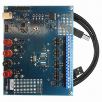
BOARD EVAL FOR CS5467 ADC
Manufacturer
Cirrus Logic Inc
Type
A/Dr
Specifications of CDB5467U
Main Purpose
Power Management, Energy/Power Meter
Embedded
Yes, MCU, 8-Bit
Utilized Ic / Part
CS5467
Primary Attributes
Watt-Hour Meter
Secondary Attributes
Graphical User Interface, SPI™ & USB Interfaces
Product
Data Conversion Development Tools
Maximum Clock Frequency
4 MHz
Interface Type
USB
Supply Voltage (max)
5 V
Supply Voltage (min)
3.3 V
For Use With/related Products
CS5467
Lead Free Status / RoHS Status
Contains lead / RoHS non-compliant
Lead Free Status / RoHS Status
Lead free / RoHS Compliant, Contains lead / RoHS non-compliant
Other names
598-1555
CDB-5467U
CDB-5467U


9.1.2 Gain Calibration
During gain calibration, a full-scale reference signal
must be applied to the meter or optionally, scaled to the
VIN1 ± ( VIN2 ±) , IIN1 ± (IIN2 ±) pins of the CS5467. A DC
reference must be used for DC gain calibration. Either
an AC or DC reference can be used for RMS AC calibra-
tions. If DC is used, the associated high-pass filter
(HPF) must be off.
Using a reference that is too large or too small can
cause an over-range condition during calibration. Either
condition can set Status register bits I1OR (I2OR)
V1OR (V2OR) for DC and I1ROR (I2ROR) V1ROR
(V2ROR) for AC calibration.
Full scale (FS) for the voltage input is ±250 mV peak
and for the current inputs is ±250 mV or ±50 mV peak
depending on selected gain range. The normal peak
voltage applied to these pins should not exceed these
levels during calibration or normal operation.
The range of the gain registers limits the gain calibration
range and subsequently the range of the reference level
that can be applied. The reference should not exceed
FS or be lower than FS/4.
9.1.2.1 AC Gain Calibration
Full scale for AC RMS gain calibrations is 60% of the in-
put’s full-scale range, which is either 250 mV or 50 mV
depending on the gain range selected. That’s 150 mV or
30 mV, again depending on range. So the normal refer-
ence input level should be either 150 or 30 mV
or DC.
Prior to executing an AC Gain Calibration command,
gain registers for any channel to be calibrated should be
set to 1.0 if the reference level mentioned above is
used, or to that level divided by the actual reference lev-
el used.
DS714F1
R eference
Figure 12
Signal
CM + -
Figure 12. System Calibration of Gain.
+
-
shows the basic setup for gain calibration.
External
Connections
IN+
IN-
+
-
XG AIN
RMS
+
-
, AC
During AC gain calibration the RMS level of the applied
reference is measured with the preset gain, then divided
into 0.6 and the quotient stored back into the corre-
sponding gain register.
9.1.2.2 DC Gain Calibration
With a DC reference applied, the DC Gain Calibration
command measures and averages DC values read on
the specified voltage or current channels and stores the
reciprocal result in the associated gain registers, con-
verting measured voltage into needed gain. Subse-
quent conversions will use the new gain value.
9.1.3 Calibration Order
1. DC offset.
2. DC or AC gain.
3. AC offset (if needed).
If both AC gain and offset calibrations were performed,
it is possible to repeat both to obtain additional accuracy
as AC gain and offset may interact.
9.1.4 Temperature Sensor Calibration
Temperature sensor calibration involves the adjustment
of two parameters -
be known in order to calibrate the temperature sensor.
See
22 for an explanation of
culate T
9.1.4.1 Temperature Offset Calibration
Offset calibration can be done at any temperature, but
should be done mid-scale if any gain error exists.
Subtract the measured T register temperature from the
actual temperature to determine the offset error. Multi-
ply this error by
V
9.1.4.2 Temperature Gain Calibration
Two temperature points far enough apart to give rea-
sonable accuracy, for example 25°C and 85°C, are re-
quired to calibrate temperature gain.
Divide the actual temperature difference by the mea-
sured ( T register) difference for the two temperatures.
This gives a gain correction factor. Update the T
register by multiplying it’s value by this correction factor.
Update
rection factor. It will be needed for subsequent offset
calibrations.
BE
0 value. Recalculate T
Section 6.13 Temperature Measurement
GAIN
∆
V
BE
and T
by dividing its old value by the gain cor-
∆
V
OFF
BE
∆
V
and add it to V
BE
register values from them.
∆
V
and V
OFF
BE
and V
using this new value .
BE
0. These values must
BE
BE
0 and how to cal-
0 to yield a new
CS5467
on page
GAIN
41
Related parts for CDB5467U
Image
Part Number
Description
Manufacturer
Datasheet
Request
R

Part Number:
Description:
Development Kit
Manufacturer:
Cirrus Logic Inc
Datasheet:
Part Number:
Description:
Development Kit
Manufacturer:
Cirrus Logic Inc
Datasheet:


Part Number:
Description:
High-efficiency PFC + Fluorescent Lamp Driver Reference Design
Manufacturer:
Cirrus Logic Inc
Datasheet:
Part Number:
Description:
Development Kit
Manufacturer:
Cirrus Logic Inc
Datasheet:
Part Number:
Description:
Development Kit
Manufacturer:
Cirrus Logic Inc
Datasheet:

Part Number:
Description:
Development Kit
Manufacturer:
Cirrus Logic Inc
Datasheet:
Part Number:
Description:
Development Kit
Manufacturer:
Cirrus Logic Inc
Datasheet:
Part Number:
Description:
Development Kit
Manufacturer:
Cirrus Logic Inc
Datasheet:
Part Number:
Description:
Development Kit
Manufacturer:
Cirrus Logic Inc
Datasheet:

Part Number:
Description:
EVALUATION BOARD FOR CS8427
Manufacturer:
Cirrus Logic Inc
Datasheet:

Part Number:
Description:
BOARD EVAL FOR CS8416 RCVR
Manufacturer:
Cirrus Logic Inc
Datasheet:

Part Number:
Description:
EVALUATION BOARD FOR CS8420
Manufacturer:
Cirrus Logic Inc
Datasheet:

Part Number:
Description:
KIT DEVELOPMENT EP9315 ARM9
Manufacturer:
Cirrus Logic Inc
Datasheet:

Part Number:
Description:
KIT DEVELOPMENT EP9302 ARM9
Manufacturer:
Cirrus Logic Inc
Datasheet: