CDB5467U Cirrus Logic Inc, CDB5467U Datasheet - Page 8
CDB5467U
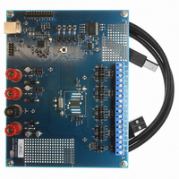
Manufacturer Part Number
CDB5467U
Description
BOARD EVAL FOR CS5467 ADC
Manufacturer
Cirrus Logic Inc
Type
A/Dr
Specifications of CDB5467U
Main Purpose
Power Management, Energy/Power Meter
Embedded
Yes, MCU, 8-Bit
Utilized Ic / Part
CS5467
Primary Attributes
Watt-Hour Meter
Secondary Attributes
Graphical User Interface, SPI™ & USB Interfaces
Product
Data Conversion Development Tools
Maximum Clock Frequency
4 MHz
Interface Type
USB
Supply Voltage (max)
5 V
Supply Voltage (min)
3.3 V
For Use With/related Products
CS5467
Lead Free Status / RoHS Status
Contains lead / RoHS non-compliant
Lead Free Status / RoHS Status
Lead free / RoHS Compliant, Contains lead / RoHS non-compliant
Other names
598-1555
CDB-5467U
CDB-5467U


ANALOG CHARACTERISTICS
Notes: 3. Applies before system calibration.
8
Analog Inputs (Voltage Inputs)
Differential Input Range
Total Harmonic Distortion
Crosstalk from Current inputs at Full Scale
Input Capacitance
Effective Input Impedance
Noise (Referred to Input)
Offset Drift (Without the High-pass Filter)
Gain Error
Temperature
Temperature Accuracy
Power Supplies
Power Supply Currents (Active State)
Power Consumption
(Note 4)
Power Supply Rejection Ratio
(Note 5)
PFMON Low-voltage Trigger Threshold
PFMON High-voltage Power-on Trip Point
4. All outputs unloaded. All inputs CMOS level.
5. Measurement method for PSRR: VREFIN tied to VREFOUT, VA+ = VD+ = 5 V, a 150 mV
6. When the voltage level on PFMON is sagging and LSD bit = 0, this is the voltage at which LSD is set to 1.
7. If the LSD bit has been set to 1 (because PFMON voltage fell below PMLO), this is the voltage level on
(zero-to-peak) (60 Hz) sinewave is imposed onto the +5 V DC supply voltage at VA+ and VD+ pins. The
“+” and “-” input pins of both input channels are shorted to AGND. The CS5467 is then commanded to
continuous conversion acquisition mode, and digital output data is collected for the channel under test.
The (zero-to-peak) value of the digital sinusoidal output signal is determined, and this value is converted
into the (zero-to-peak) value of the sinusoidal voltage (measured in mV) that would need to be applied
at the channel’s inputs, in order to cause the same digital sinusoidal output. This voltage is then defined
as Veq. PSRR is (in dB)
PFMON at which the LSD bit can be permanently reset back to 0.
Parameter
Active State (VA+ = 5 V, VD+ = 3.3 V)
(50, 60 Hz)
Active State (VA+ = VD+ = 5 V)
I
D+
:
(VA+ = 5 V, VD+ = 3.3 V)
Current
Current
I
D+
(Continued)
(VA+ = VD+ = 5 V)
[(VIN+) – (VIN-)]
All Gain Ranges
Stand-by State
PSRR
(Gain = 50x)
(Gain = 10x)
Sleep State
(50, 60 Hz)
Voltage
(Note 3)
(Note 6)
(Note 7)
=
I
20
A+
⋅
log
Symbol
PMLO
PSCA
PSCD
PSCD
PSRR
PMHI
THD
VIN
OD
GE
PC
EII
N
IC
150
--------- -
V
T
V
eq
Min
2.3
65
48
68
60
2
-
-
-
-
-
-
-
-
-
-
-
-
-
-
-
16.0
±3.0
2.45
2.55
Typ
500
-70
2.0
1.5
3.5
2.3
75
±5
25
15
10
55
75
65
7
-
-
Max
140
2.7
33
20
-
-
-
-
-
-
-
-
-
-
-
-
-
-
-
-
CS5467
DS714F1
mV
µV/°C
µV
Unit
mW
mW
mW
MΩ
mA
mA
mA
uW
dB
dB
dB
dB
dB
pF
°C
%
V
V
rms
P-P
Related parts for CDB5467U
Image
Part Number
Description
Manufacturer
Datasheet
Request
R

Part Number:
Description:
Development Kit
Manufacturer:
Cirrus Logic Inc
Datasheet:
Part Number:
Description:
Development Kit
Manufacturer:
Cirrus Logic Inc
Datasheet:


Part Number:
Description:
High-efficiency PFC + Fluorescent Lamp Driver Reference Design
Manufacturer:
Cirrus Logic Inc
Datasheet:
Part Number:
Description:
Development Kit
Manufacturer:
Cirrus Logic Inc
Datasheet:
Part Number:
Description:
Development Kit
Manufacturer:
Cirrus Logic Inc
Datasheet:

Part Number:
Description:
Development Kit
Manufacturer:
Cirrus Logic Inc
Datasheet:
Part Number:
Description:
Development Kit
Manufacturer:
Cirrus Logic Inc
Datasheet:
Part Number:
Description:
Development Kit
Manufacturer:
Cirrus Logic Inc
Datasheet:
Part Number:
Description:
Development Kit
Manufacturer:
Cirrus Logic Inc
Datasheet:

Part Number:
Description:
EVALUATION BOARD FOR CS8427
Manufacturer:
Cirrus Logic Inc
Datasheet:

Part Number:
Description:
BOARD EVAL FOR CS8416 RCVR
Manufacturer:
Cirrus Logic Inc
Datasheet:

Part Number:
Description:
EVALUATION BOARD FOR CS8420
Manufacturer:
Cirrus Logic Inc
Datasheet:

Part Number:
Description:
KIT DEVELOPMENT EP9315 ARM9
Manufacturer:
Cirrus Logic Inc
Datasheet:

Part Number:
Description:
KIT DEVELOPMENT EP9302 ARM9
Manufacturer:
Cirrus Logic Inc
Datasheet: