AD9551/PCBZ Analog Devices Inc, AD9551/PCBZ Datasheet - Page 16
AD9551/PCBZ
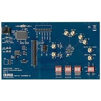
Manufacturer Part Number
AD9551/PCBZ
Description
BOARD EVAL FOR AD9951
Manufacturer
Analog Devices Inc
Datasheet
1.AD9551PCBZ.pdf
(40 pages)
Specifications of AD9551/PCBZ
Main Purpose
Timing, Clock Generator
Embedded
No
Utilized Ic / Part
AD9551
Primary Attributes
2 Inputs, 2 Outputs, VCO
Secondary Attributes
Graphical User Interface, USB Interface
Silicon Manufacturer
Analog Devices
Application Sub Type
Clock Generator
Kit Application Type
Clock & Timing
Silicon Core Number
AD9551
Kit Contents
Board
Lead Free Status / RoHS Status
Lead free / RoHS Compliant


AD9551
THEORY OF OPERATION
OPERATING MODES
The AD9551 provides the following fundamental operating modes:
•
•
Mode selection depends on the state of the frequency selection pins
(A[3:0] and B[3:0]). If all four of the A[3:0] pins or all four of
the B[3:0] pins are Logic 1s, the 19.44 MHz mode is in effect.
Otherwise, normal mode is in effect.
Normal Mode
Normal mode offers two methods of operation. The first method
relies on the frequency selection pins to configure the device.
The second method involves the use of the serial port for device
configuration.
The first method is for applications that use one of the input/output
frequency sets defined in Table 13 and Table 14 (excluding the
19.44 MHz mode selection). The advantage of this method is
that the serial port is not required. Connect the pins to the appro-
priate logic levels, and the device operates with the defined input
and output frequencies. The pin settings establish all the necessary
internal divider values. Note, however, that this method requires an
external crystal with a resonant frequency of 26 MHz.
The second method, which relies on the serial port, enables the
user to program custom divider settings to achieve input/output
frequency ratios not available via the frequency selection pins.
Furthermore, the 26 MHz constraint on the external crystal no
longer applies. Note, however, that the external pin settings still
establish the default values of the dividers. The serial port simply
enables the user to override the default settings.
19.44 MHz Mode
This special operating mode allows for input references that
operate specifically at 19.44 MHz, 38.88 MHz, or 77.76 MHz.
The 19.44 MHz mode is invoked by the frequency selection pins
and occurs when either A[3:0] = 1111b or B[3:0] = 1111b. Fur-
thermore, this mode requires an external crystal with one of the
following four possible resonant frequencies, based on the contents
of Register 0x33[5:4].
•
•
•
•
In the 19.44 MHz mode, the reference input dividers allow for
integer divide ratios of 1, 2, or 4 only, set via Register 0x1E[1:0].
Therefore, if f
if f
77.76 MHz, the divide ration must be set to 4.
Note that for applications using both REFA and REFB in the
19.44 MHz mode, the input frequencies must match.
IN
Normal mode
19.44 MHz mode
49.152 MHz
49.860 MHz
50.000 MHz
52.000 MHz
= 38.88 MHz, the divide ratio must be set to 2; and if f
IN
= 19.44 MHz, the divide ratio must be set to 1;
IN
Rev. B | Page 16 of 40
=
Although the 19.44 MHz mode limits the input divide ratio to
1, 2, or 4, the user has full control of the dividers in the output
section. This includes the integer and fractional components of
the output PLL feedback divider and the final output dividers
(P
frequencies.
Note that the 19.44 MHz mode alters the configuration of the input
PLL (see the Input PLL section).
When using the 19.44 MHz mode, the loop filter in the output PLL
requires a 100 nF capacitor. Furthermore, the user must program
the output PLL charge pump current to 25 μA (via Register 0x0A).
Note that SPI port programming capability is necessary when
using 19.44 MHz mode because it requires a charge pump current
that is different from the default value.
COMPONENT BLOCKS
Input Dividers
Each reference input feeds a dedicated reference divider block.
The input dividers provide division of the reference frequency
in integer steps from 1 to 63. They provide the bulk of the fre-
quency prescaling necessary to reduce the reference frequency
to accommodate the bandwidth limitations of both the input
and output PLLs.
Input Sigma-Delta Modulators (SDM)
Each of the two input dividers is coupled with an optional, second-
order SDM, enabling fractional division of the input reference
frequency. With both integer and fractional divide capability, the
AD9551 can accept two different reference frequencies that span
a wide range of possible input frequency ratios.
A typical SDM offers fractional division in the form N + F/M,
where N is the integer part, M is the modulus, and F is the frac-
tional part (F < M). All three parameters are positive integers. The
input SDMs of the AD9551 are atypical in that they implement
fractional division in the form, N + 1/2 + F/(2M), with F being
a signed integer, and |F| < M. Note that when the SDM is in use,
the minimum integer divide value is 4.
Both SDMs have an integrated pseudorandom binary sequence
(PRBS) generator. The PRBS generator serves to suppress spurious
artifacts by adding a random component to the SDM output. By
default, the PRBS generator is active in both input SDMs, but
the user can disable the PRBS using Register 0x1E[2].
Note that in 19.44 MHz mode, the input SDMs are inactive and
unavailable.
Reference Monitor
The reference monitor verifies the presence or absence of the
prescaled REFA and REFB signals (that is, after division by the
input dividers). The status of the reference monitor guides the
activity of the synchronization and switchover control logic.
Note that the DCXO must be operational for the reference
monitor to function.
0
, P
1
, and P
2
), enabling the synthesis of a wide range of output
Related parts for AD9551/PCBZ
Image
Part Number
Description
Manufacturer
Datasheet
Request
R


Part Number:
Description:
±1.7g Dual-Axis IMEMS Accelerometer Evaluation Board
Manufacturer:
Analog Devices Inc
Datasheet:

Part Number:
Description:
Inertial Sensor Evaluation System
Manufacturer:
Analog Devices Inc
Datasheet:
Part Number:
Description:
Manufacturer:
Analog Devices Inc
Datasheet:
Part Number:
Description:
Manufacturer:
Analog Devices Inc
Datasheet:
Part Number:
Description:
Manufacturer:
Analog Devices Inc
Datasheet:
Part Number:
Description:
Manufacturer:
Analog Devices Inc
Datasheet:
Part Number:
Description:
Manufacturer:
Analog Devices Inc
Datasheet:
Part Number:
Description:
Manufacturer:
Analog Devices Inc
Datasheet:
Part Number:
Description:
Manufacturer:
Analog Devices Inc
Datasheet:
Part Number:
Description:
Manufacturer:
Analog Devices Inc
Datasheet:
Part Number:
Description:
Manufacturer:
Analog Devices Inc
Datasheet:
Part Number:
Description:
Manufacturer:
Analog Devices Inc
Datasheet: