AD9551/PCBZ Analog Devices Inc, AD9551/PCBZ Datasheet - Page 21
AD9551/PCBZ
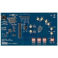
Manufacturer Part Number
AD9551/PCBZ
Description
BOARD EVAL FOR AD9951
Manufacturer
Analog Devices Inc
Datasheet
1.AD9551PCBZ.pdf
(40 pages)
Specifications of AD9551/PCBZ
Main Purpose
Timing, Clock Generator
Embedded
No
Utilized Ic / Part
AD9551
Primary Attributes
2 Inputs, 2 Outputs, VCO
Secondary Attributes
Graphical User Interface, USB Interface
Silicon Manufacturer
Analog Devices
Application Sub Type
Clock Generator
Kit Application Type
Clock & Timing
Silicon Core Number
AD9551
Kit Contents
Board
Lead Free Status / RoHS Status
Lead free / RoHS Compliant


HOLDOVER MODE
In the absence of both input references, the device enters holdover
mode. Holdover is a secondary function that is provided by the
input PLL. Because the DCXO has an external crystal as its fre-
quency source, it continues to operate in the absence of the input
reference signals. When the device switches to holdover, the DCXO
is held at the frequency at which it was operating just prior to
switchover. The device continues operating in this mode until
a reference signal becomes available; the device then exits holdover
mode, and the input PLL resynchronizes with the active reference.
JITTER TOLERANCE
Jitter tolerance is the ability of the AD9551 to maintain lock in the
presence of sinusoidal jitter. The AD9551 meets the DS1 reference
input jitter tolerance mask per Telcordia GR-1244-CORE (see
Figure 22). The acceptable jitter tolerance is the region above the
mask.
EXTERNAL LOOP FILTER CAPACITOR
The output PLL loop filter requires the connection of an external
capacitor from LF (Pin 17) to LDO_VCO (Pin 22). The value of
the external capacitor depends on the operating mode (normal
or 19.44 MHz). Normal mode requires a 12 nF capacitor that sets
the loop bandwidth at approximately 70 kHz and ensures loop
stability over the intended operating parameters of the device.
The 19.44 MHz mode requires a 100 nF capacitor, along with
a change in the output PLL charge pump current to 25 μA, via
Register 0x0A. This establishes similar loop bandwidth and
stability criteria as found in normal mode.
Note that the 19.44 MHz mode does not function properly
unless the user changes the output PLL charge pump current
from its default setting to 25 μA.
OUTPUT/INPUT FREQUENCY RELATIONSHIP
Following are the three equations that define the frequency
at OUT1 and OUT2 (f
in the equations throughout this datasheet, the subscripted x
indicates A or B.
0.1
10
1
10
EXTERNAL TIMING MASK
100
Figure 22. Jitter Tolerance
OUT1
JITTER FREQUENCY (Hz)
and f
OUT2
1k
, respectively). Note that
LINE TIMING MASK
10k
100k
Rev. B | Page 21 of 40
where:
f
subscripted A or B indicating REFA or REFB, respectively.
f
P
P
K is the input mode scale factor.
N
divider values, with the A or B subscript indicating REFA or REFB,
respectively.
N, FRAC, and MOD are the feedback divider values for the
output PLL.
The various dividers have the following constraints:
The VCO imposes the following constraint on f
The input frequencies (f
relationship:
N
N
FRAC
FRAC
P
P
P
MOD
N ∈
MOD ∈
REF
IF
0
2
A
0
1
2
is the frequency at the input of the output PLL’s PDF.
x
x
and P
is the OUT2 divider value.
, N
∈
∈
∈
A
∈
∈
and f
{
{
{
{
B
f
f
1
⎛
⎜
⎜
⎝
N
f
1
{
{
64
4
, FRAC
x
OUT1
OUT2
, 1 L
, 3 L
x
IF
∈
, 2 ,
, 2 ,
N
, 5 ,
∈
A
∈ −
1
, 2
, 4
{
,
{
3350
0 L
L
are OUT1 divider values.
, 1
L
+
=
{
+
REF
{
65
L
, 1 L
, 1 ,
=
=
FRAC
⎛
⎜ ⎜
⎝
, 2
MOD
,
,
f
, 2
B
,
524
63
,
A
,
63
11
1
2
,
REF
f
63
, FRAC
L
f
are the input reference frequency, with the
63
L
IF
OUT1
f
P
}
+
}
}
, 1 ,
}
REF
⎛
⎜
⎜
⎝
2
}
,
⎞
⎟
⎟
⎠
,
x
288
,
, 1 ,
( 2
524
N
255
048
with SDM disabled
MHz
⎛
⎜
⎜
⎜
⎜
⎜
⎝
with SDM active
FRAC
A
N
048
MOD
P
+
B
,
0
,
,
, MOD
−
}
287
x
575
P
FRAC
MOD
524
1
,
+
≤
REF
575
}
}
⎛
⎜
⎜
⎝
A
A
f
A
,
1
2
⎞
⎟
⎟
⎠
IF
287
)
}
A
and f
⎞
⎟ ⎟
⎠
, and MOD
+
≤
K
=
( 2
,
⎛
⎜
⎜
⎝
L
FRAC
N
REF
N
MOD
,
4050
524
+
B
B
) must satisfy the following
FRAC
+
MOD
,
287
⎛
⎜ ⎜
⎝
x
B
x
1
2
)
are the input reference
⎞
⎟
⎟
⎠
⎞
⎟
⎟
⎠
f
}
+
MHz
REF
⎞
⎟
⎟
⎟
⎟
⎟
⎠
2
FRAC
(
B
IF
MOD
:
AD9551
B
B
)
⎞
⎟ ⎟
⎠
1)
2)
3)
Related parts for AD9551/PCBZ
Image
Part Number
Description
Manufacturer
Datasheet
Request
R


Part Number:
Description:
±1.7g Dual-Axis IMEMS Accelerometer Evaluation Board
Manufacturer:
Analog Devices Inc
Datasheet:

Part Number:
Description:
Inertial Sensor Evaluation System
Manufacturer:
Analog Devices Inc
Datasheet:
Part Number:
Description:
Manufacturer:
Analog Devices Inc
Datasheet:
Part Number:
Description:
Manufacturer:
Analog Devices Inc
Datasheet:
Part Number:
Description:
Manufacturer:
Analog Devices Inc
Datasheet:
Part Number:
Description:
Manufacturer:
Analog Devices Inc
Datasheet:
Part Number:
Description:
Manufacturer:
Analog Devices Inc
Datasheet:
Part Number:
Description:
Manufacturer:
Analog Devices Inc
Datasheet:
Part Number:
Description:
Manufacturer:
Analog Devices Inc
Datasheet:
Part Number:
Description:
Manufacturer:
Analog Devices Inc
Datasheet:
Part Number:
Description:
Manufacturer:
Analog Devices Inc
Datasheet:
Part Number:
Description:
Manufacturer:
Analog Devices Inc
Datasheet: