AD9551/PCBZ Analog Devices Inc, AD9551/PCBZ Datasheet - Page 3
AD9551/PCBZ
Manufacturer Part Number
AD9551/PCBZ
Description
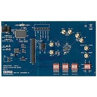
BOARD EVAL FOR AD9951
Manufacturer
Analog Devices Inc
Datasheet
1.AD9551PCBZ.pdf
(40 pages)
Specifications of AD9551/PCBZ
Main Purpose
Timing, Clock Generator
Embedded
No
Utilized Ic / Part
AD9551
Primary Attributes
2 Inputs, 2 Outputs, VCO
Secondary Attributes
Graphical User Interface, USB Interface
Silicon Manufacturer
Analog Devices
Application Sub Type
Clock Generator
Kit Application Type
Clock & Timing
Silicon Core Number
AD9551
Kit Contents
Board
Lead Free Status / RoHS Status
Lead free / RoHS Compliant


REFA, REFA
REFB, REFB
SCLK, SDIO,
The AD9551 is easily configured using the external control pins
(A[3:0], B[3:0], and Y[3:0]). The logic state of these pins sets pre-
defined divider values that establish a specific input-to-output
frequency ratio. For applications requiring other frequency ratios,
the user can override any of the preconfigured divider settings
via the serial port, which enables a very wide range of
applications.
The AD9551 architecture consists of two cascaded PLL stages.
The first stage consists of fractional division (via SDM), followed
by a digital PLL that uses a crystal resonator-based DCXO. The
DCXO relies on an external crystal with a resonant frequency in
the range of 19.44 MHz to 52 MHz. The DCXO constitutes the
first PLL, which operates within a narrow frequency range
(±50 ppm) around the crystal resonant frequency. This PLL has
a loop bandwidth of approximately 180 Hz, providing initial jitter
cleanup of the input reference signal. The second stage is a fre-
quency multiplying PLL that translates the first stage output
frequency (in the range of 19.44 MHz to 104 MHz) up to
~3.7 GHz. This PLL incorporates an SDM-based fractional
feedback divider that enables fractional frequency multiplication.
Programmable integer dividers at the output of this second PLL
establish a final output frequency of up to 900 MHz.
It is important to understand that the architecture of the AD9551
produces an output frequency that is most likely not coherent
with the input reference frequency. The reason is that the input
and crystal frequencies typically are not harmonically related
and neither are the output and crystal frequencies. As a result,
there is generally no relationship between the phase of the input
and output signals.
A[3:0]
B[3:0]
Y[3:0]
CS
2
2
f
f
REFB
REFA
3
4
4
4
SDM
SDM
N
N
PRECONFIGURED
REGISTER BANK
DIVIDER VALUES
A
B
A
B
REFERENCE
MONITOR
SAMPLE RATE
CONTROL
19.44MHz MODE
INPUT PLL
LOCKED
P
D
F
FILTER
LOOP
DIG.
FUNCTIONAL BLOCK DIAGRAM
XTAL1 XTAL0
N
N
N, MOD, FRAC, P
DCXO
A
B
, MOD
, MOD
A
B
CONFIGURATION
19.44MHz MODE
, FRAC
, FRAC
Rev. B | Page 3 of 40
LOOP
A
B
0
Figure 2.
, P
1
, P
2
OUTPUT PLL
The AD9551 includes reference signal processing blocks that
enable a smooth switching transition between two reference
inputs. This circuitry automatically detects the presence of the
reference input signals. If only one input is present, the device
uses it as the active reference. If both inputs are present, one
becomes the active reference and the other becomes the alter-
nate reference. The circuitry edge-aligns the backup reference
with the active reference. If the active reference fails, the circuitry
automatically switches to the backup reference (if available),
making it the new active reference. Meanwhile, if the failed
reference is once again available, it becomes the new backup
reference and is edge-aligned with the new active reference
(a precaution against failure of the new active reference).
If neither reference can be used, the AD9551 supports a holdover
mode. Note that the external crystal is necessary to provide the
switchover and holdover functionality. It is also the clock source
for the reference synchronization and monitoring functions.
The AD9551 relies on a single external capacitor for the output
PLL loop filter. With proper termination, the output is compatible
with LVPECL, LVDS, or CMOS logic levels, although the AD9551
is implemented in a strictly CMOS process.
The AD9551 operates over the extended industrial temperature
range of −40°C to +85°C.
LOCKED
TEST
MUX
f
DETECT
IF
LOCK
P
F
D
N = 4N
CHARGE
N1
PUMP
SDM
1
+ N
4/5
LF
0
3350MHz TO
4050MHz
VCO
N
P
2
, P
1
, P
0
4 TO
11
P
0
AD9551
1 TO
63
P
1 TO
1
63
P
2
f
f
OUT1
OUT2
2
2
AD9551
OUT1, OUT1
OUT2, OUT2
Related parts for AD9551/PCBZ
Image
Part Number
Description
Manufacturer
Datasheet
Request
R


Part Number:
Description:
±1.7g Dual-Axis IMEMS Accelerometer Evaluation Board
Manufacturer:
Analog Devices Inc
Datasheet:

Part Number:
Description:
Inertial Sensor Evaluation System
Manufacturer:
Analog Devices Inc
Datasheet:
Part Number:
Description:
Manufacturer:
Analog Devices Inc
Datasheet:
Part Number:
Description:
Manufacturer:
Analog Devices Inc
Datasheet:
Part Number:
Description:
Manufacturer:
Analog Devices Inc
Datasheet:
Part Number:
Description:
Manufacturer:
Analog Devices Inc
Datasheet:
Part Number:
Description:
Manufacturer:
Analog Devices Inc
Datasheet:
Part Number:
Description:
Manufacturer:
Analog Devices Inc
Datasheet:
Part Number:
Description:
Manufacturer:
Analog Devices Inc
Datasheet:
Part Number:
Description:
Manufacturer:
Analog Devices Inc
Datasheet:
Part Number:
Description:
Manufacturer:
Analog Devices Inc
Datasheet:
Part Number:
Description:
Manufacturer:
Analog Devices Inc
Datasheet: