AD9551/PCBZ Analog Devices Inc, AD9551/PCBZ Datasheet - Page 4
AD9551/PCBZ
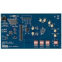
Manufacturer Part Number
AD9551/PCBZ
Description
BOARD EVAL FOR AD9951
Manufacturer
Analog Devices Inc
Datasheet
1.AD9551PCBZ.pdf
(40 pages)
Specifications of AD9551/PCBZ
Main Purpose
Timing, Clock Generator
Embedded
No
Utilized Ic / Part
AD9551
Primary Attributes
2 Inputs, 2 Outputs, VCO
Secondary Attributes
Graphical User Interface, USB Interface
Silicon Manufacturer
Analog Devices
Application Sub Type
Clock Generator
Kit Application Type
Clock & Timing
Silicon Core Number
AD9551
Kit Contents
Board
Lead Free Status / RoHS Status
Lead free / RoHS Compliant


AD9551
SPECIFICATIONS
Minimum and maximum values apply for full range of supply voltage and operating temperature variation. Typical values apply for VDD = 3.3 V,
T
REFERENCE CLOCK INPUT CHARACTERISTICS
Table 1.
Parameter
FREQUENCY RANGE
INPUT CAPACITANCE
INPUT RESISTANCE
DUTY CYCLE
REFERENCE CLOCK INPUT VOLTAGE SWING
1
OUTPUT CHARACTERISTICS
Table 2.
Parameter
LVPECL MODE
LVDS MODE
CMOS MODE
The 19 MHz lower limit applies only to the 19.44 MHz operating mode.
A
Differential
Single-Ended
Differential Output Voltage Swing
Common-Mode Output Voltage
Frequency Range
Duty Cycle
Rise/Fall Time
Differential Output Voltage Swing
Offset Voltage
Short-Circuit Output Current
Frequency Range
Duty Cycle
Rise/Fall Time
Output Voltage High, V
Output Voltage Low, V
Frequency Range
= 25°C, unless otherwise noted.
Balanced, V
Unbalanced, ΔV
Common Mode, V
Common-Mode Difference, ΔV
I
I
I
I
OH
OH
OL
OL
= 10 mA
= 1 mA
= 10 mA
= 1 mA
1
1
OD
(20% to 80%)
(20% to 80%)
OD
OS
OL
OH
OS
250
690
VDD − 1.77
247
1.125
Min
19
40
250
Min
0
40
0
40
2.8
2.8
0
1
Typ
3
6
Typ
765
VDD − 1.66
17
255
285
Rev. B | Page 4 of 40
Max
806
60
Max
889
VDD − 1.20
900
60
305
454
25
1.375
25
24
900
60
355
0.5
0.3
200
Unit
MHz
pF
kΩ
%
mV
mV
Unit
mV
V
MHz
%
ps
mV
mV
V
mV
mA
MHz
%
ps
V
V
V
V
MHz
Test Conditions/Comments
Measured single-ended
Measured with a differential probe across
the input pins
Maximum magnitude across pin pair
Peak-to-peak
Test Conditions/Comments
Output driver static
Output driver static
Up to 805 MHz output frequency
100 Ω termination between both pins of
the output driver
Voltage swing between output pins;
output driver static
Absolute difference between voltage
swing of normal pin and inverted pin;
output driver static
Output driver static
Voltage difference between output pins;
output driver static
Up to 805 MHz output frequency
100 Ω termination between both pins of
the output driver
Output driver static; standard drive
strength setting
Output driver static; standard drive
strength setting
3.3 V CMOS; standard drive strength
setting
Related parts for AD9551/PCBZ
Image
Part Number
Description
Manufacturer
Datasheet
Request
R


Part Number:
Description:
±1.7g Dual-Axis IMEMS Accelerometer Evaluation Board
Manufacturer:
Analog Devices Inc
Datasheet:

Part Number:
Description:
Inertial Sensor Evaluation System
Manufacturer:
Analog Devices Inc
Datasheet:
Part Number:
Description:
Manufacturer:
Analog Devices Inc
Datasheet:
Part Number:
Description:
Manufacturer:
Analog Devices Inc
Datasheet:
Part Number:
Description:
Manufacturer:
Analog Devices Inc
Datasheet:
Part Number:
Description:
Manufacturer:
Analog Devices Inc
Datasheet:
Part Number:
Description:
Manufacturer:
Analog Devices Inc
Datasheet:
Part Number:
Description:
Manufacturer:
Analog Devices Inc
Datasheet:
Part Number:
Description:
Manufacturer:
Analog Devices Inc
Datasheet:
Part Number:
Description:
Manufacturer:
Analog Devices Inc
Datasheet:
Part Number:
Description:
Manufacturer:
Analog Devices Inc
Datasheet:
Part Number:
Description:
Manufacturer:
Analog Devices Inc
Datasheet: