AD9551/PCBZ Analog Devices Inc, AD9551/PCBZ Datasheet - Page 6
AD9551/PCBZ
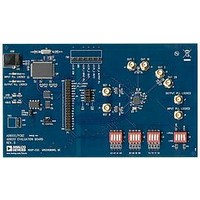
Manufacturer Part Number
AD9551/PCBZ
Description
BOARD EVAL FOR AD9951
Manufacturer
Analog Devices Inc
Datasheet
1.AD9551PCBZ.pdf
(40 pages)
Specifications of AD9551/PCBZ
Main Purpose
Timing, Clock Generator
Embedded
No
Utilized Ic / Part
AD9551
Primary Attributes
2 Inputs, 2 Outputs, VCO
Secondary Attributes
Graphical User Interface, USB Interface
Silicon Manufacturer
Analog Devices
Application Sub Type
Clock Generator
Kit Application Type
Clock & Timing
Silicon Core Number
AD9551
Kit Contents
Board
Lead Free Status / RoHS Status
Lead free / RoHS Compliant


AD9551
LOGIC INPUT PINS
Table 6.
Parameter
INPUT CHARACTERISTICS
1
RESET PIN
Table 7.
Parameter
INPUT CHARACTERISTICS
MINIMUM PULSE WIDTH HIGH
1
LOGIC OUTPUT PINS
Table 8.
Parameter
OUTPUT CHARACTERISTICS
SERIAL CONTROL PORT
Table 9.
Parameter
CS
SCLK
SDIO
The A[3:0], B[3:0], Y[3:0], and OUTSEL pins have 100 kΩ internal pull-up resistors.
The RESET pin has a 100 kΩ internal pull-up resistor, so the default state of the device is reset.
Logic 1 Voltage, V
Logic 0 Voltage, V
Logic 1 Current, I
Logic 0 Current, I
Input Voltage High, V
Input Voltage Low, V
Input Current High, I
Input Current Low, I
Output Voltage High, V
Output Voltage Low, V
Input Logic 1 Voltage
Input Logic 0 Voltage
Input Logic 1 Current
Input Logic 0 Current
Input Capacitance
Input Logic 1 Voltage
Input Logic 0 Voltage
Input Logic 1 Current
Input Logic 0 Current
Input Capacitance
Input
Input Logic 1 Voltage
Input Logic 0 Voltage
IH
IL
IH
IL
INL
IL
INH
IH
OL
1
1
OH
Min
1.0
Min
1.8
2
Min
2.7
Min
1.6
1.6
1.6
Typ
Typ
2
2
2
2
Typ
0.3
31
Typ
Rev. B | Page 6 of 40
Max
0.8
3
17
Max
1.3
12.5
43
Max
0.4
Max
0.5
0.03
0.5
0.03
0.5
Unit
V
V
μA
μA
pF
V
V
μA
μA
pF
V
V
Unit
V
V
μA
μA
Unit
V
V
μA
μA
ns
Unit
V
V
Test Conditions/Comments
For the CMOS inputs, a static Logic 1 results
from either a pull-up resistor or no connection
Test Conditions/Comments
Related parts for AD9551/PCBZ
Image
Part Number
Description
Manufacturer
Datasheet
Request
R


Part Number:
Description:
±1.7g Dual-Axis IMEMS Accelerometer Evaluation Board
Manufacturer:
Analog Devices Inc
Datasheet:

Part Number:
Description:
Inertial Sensor Evaluation System
Manufacturer:
Analog Devices Inc
Datasheet:
Part Number:
Description:
Manufacturer:
Analog Devices Inc
Datasheet:
Part Number:
Description:
Manufacturer:
Analog Devices Inc
Datasheet:
Part Number:
Description:
Manufacturer:
Analog Devices Inc
Datasheet:
Part Number:
Description:
Manufacturer:
Analog Devices Inc
Datasheet:
Part Number:
Description:
Manufacturer:
Analog Devices Inc
Datasheet:
Part Number:
Description:
Manufacturer:
Analog Devices Inc
Datasheet:
Part Number:
Description:
Manufacturer:
Analog Devices Inc
Datasheet:
Part Number:
Description:
Manufacturer:
Analog Devices Inc
Datasheet:
Part Number:
Description:
Manufacturer:
Analog Devices Inc
Datasheet:
Part Number:
Description:
Manufacturer:
Analog Devices Inc
Datasheet: