ADNK-5053-HT01 Avago Technologies US Inc., ADNK-5053-HT01 Datasheet
ADNK-5053-HT01
Specifications of ADNK-5053-HT01


Related parts for ADNK-5053-HT01


ADNK-5053-HT01 Summary of contents
Page 1
ADNS-5050 Optical Mouse Sensor Data Sheet Description The ADNS-5050 is a mainstream, small form factor optical mouse sensor user-friendly product with many built-in features and optimized for LED-based corded products. The ADNS-5050 is capable of high-speed motion ...
Page 2
Pinout of ADNS-5050 Optical Mouse Sensor Pin Name Description 1 SDIO Serial Port Data Input and Output 2 XY_LED LED Control 3 NRESET Reset Pin (active low input) 4 NCS Chip Select (active low input Supply Voltage DD5 ...
Page 3
Overview of Optical Mouse Sensor Assembly Avago Technologies provides an IGES file drawing de- scribing the base plate molding features for lens and PCB alignment. The ADNS-5050 sensor is designed for mounting on a through-hole PCB, looking down. There is ...
Page 4
DIMENSIONS IN mm (INCHES) 7.45 10.58 10.58 TOP PCB to SURFACE (0.293) (0.417) (0.417) 2.40 BOTTOM of LENS FLANGE to SURFACE (0.094) Figure 4. 2D Assembly drawing of ADNS-5050 (top and side views). 4 33.45 (1.317) TOP VIEW CROSS SECTION ...
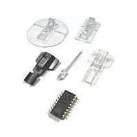
Page 5
ADNS-5200 (LED CLIP) SENSOR CUSTOMER SUPPLIED BASE PLATE WITH RECOMMENDED ALIGNMENT FEATURES PER IGES DRAWING Figure 5. Exploded view drawing. PCB Assembly Considerations 1. Insert the sensor and all other electrical components into PCB. 2. Insert the LED into the ...
Page 6
Design Considerations for Improved ESD Performance For improved electrostatic discharge performance, typical creepage and clearance distance are shown in the table below. Assumption: base plate construction as per the Avago Technologies supplied IGES file and ADNS-5100/5100-001 lens. Typical Distance A5100 ...
Page 7
SW2 SW1 SW3 P1.0 P1.1 P1.2 VCC P1.3 P1.6 P1 VBUS 2 GND D+/SCLK D+ 3 D-/SDAT D- 4 POWER R13 P1.5 1.30K XOUT VREG XIN/P2.1 Figure 8. Schematic diagram for interface between ADNS-5050 and microcontroller. 7 MIDDLE ...
Page 8
Regulatory Requirements • Passes FCC B and worldwide analogous emission limits when assembled into a mouse with shielded cable and following Avago Technologies recommendations. • Passes IEC-1000-4-3 radiated susceptibility level when assembled into a mouse with shielded cable and following ...
Page 9
AC Electrical Specifications Electrical Characteristics over recommended operating conditions. Typical values at 25 °C, V Parameter Symbol Power Down t PD Wake from Power Down t WAKEUP Reset Pulse Width t RESET Motion Delay after Reset t MOT-RST SDIO Rise ...
Page 10
DC Electrical Specifications Electrical Characteristics over recommended operating conditions. Typical values at 25 °C, V Parameter Symbol DC Supply Current I DD_AVG Idle Supply Current I DD_IDLE Power Down Supply Current I DD_PD Input Low Voltage V IL Input High ...
Page 11
Typical Performance Characteristics 1200 1000 1200 800 1000 600 800 400 600 200 400 0 200 1.6 1.7 1.8 1 1.6 1.7 1.8 1.9 2 Figure 10. Mean resolution vs. distance from lens reference plane to surface. 25 ...
Page 12
LED Mode For optimized tracking performance, the LED mode when motion is detected, and ADNS-5050 will pulse the LED when the mouse is in idle state. To force the LED into always DC mode, kindly refer to ...
Page 13
Read Operation A read operation, defined as data going from the ADNS-5050 to the micro-controller, is always initiated by the micro- controller and consists of two bytes. The first byte contains the address, is sent by the micro-controller over SDIO, ...
Page 14
Required Timing between Read and Write Commands There are minimum timing requirements between read and write commands on the serial port. SCLK ADDRESS DATA WRITE OPERATION Timing between Two Write Commands If the rising edge of the SCLK for the ...
Page 15
Motion Burst Timing SCLK MOTION_BURST REGISTER ADDRESS READ FIRST BYTE FIRST READ OPERATION Burst Mode Operation Burst mode is a special serial port operation mode that may be used to reduce the serial transaction time for a motion read. The ...
Page 16
Registers The ADNS-5050 registers are accessible via the serial port. The registers are used to read motion data and status as well as to set the device configuration. Address Register 0x00 Product_ID 0x01 Revision_ID 0x02 Motion 0x03 Delta_X 0x04 Delta_Y ...
Page 17
Product_ID Address: 0x00 Access: Read Reset Value: 0x12 Bit 7 Field PID 7 Data Type: 8-Bit unsigned integer USAGE: This register value is made to be the same as ADNS-5020-EN for direct replacement. The alternative PID is located at Product_ID2 ...
Page 18
Delta_X Address: 0x03 Access: Read Reset Value: 0x00 Bit 7 Field X 7 Data Type: Eight bit 2’s complement number. USAGE: X movement is counts since last report. Absolute value is determined by resolution. Reading clears the register. MOTION -128 ...
Page 19
SQUAL Address: 0x05 Access: Read Reset Value: 0x00 Bit 7 Field SQ 7 Data Type: Upper 8 bits of a 9-bit unsigned integer. USAGE: SQUAL (Surface Quality measure of the number of valid features visible by the sensor ...
Page 20
Shutter_Upper Address: 0x06 Access: Read Reset Value: 0x00 Bit 7 Field S 15 Shutter_Lower Address: 0x07 Access: Read Reset Value: 0x00 Bit 7 Field S 7 Data Type: Sixteen bit unsigned integer. USAGE: Units are clock cycles. They must be ...
Page 21
Maximum_Pixel Address: 0x08 Access: Read Reset Value: 0x00 Bit 7 Field MP 0 Data Type: Seven-bit number. USAGE: Maximum Pixel value in current frame. Minimum value = 0, maximum value = 127. The maximum pixel value can vary with every ...
Page 22
Pixel_Grab Address: 0x0b Access: Read/Write Reset Value: 0x00 Bit 7 Field Valid Data Type: Eight-bit word. USAGE: The pixel grabber captures 1 pixel per frame. If there is a valid pixel in the grabber when this register is read, the ...
Page 23
Reserved Address: 0x0c Mouse_control Address: 0x0d Access: Read/Write Reset Value: 0x00 Bit 7 Field Reserved Reserved Reserved Reserved Reserved Reserved PD Data Type: Eight bit number USAGE: Resolution and Power Down information can be accessed edited by ...
Page 24
Reserved Address: 0x0e-0x18 Mouse_Control2 Address: 0x19 Access: Write Reset Value: 0x08 Bit 7 Field Reserved Reserved Reserved RES_EN Data Type: Eight bit number USAGE: Resolution information can be accessed edited by this register. Field Name RES_EN RES ...
Page 25
Reserved Address: 0x1a-0x21 LED_DC_Mode Address: 0x22 Access: Read/Write Reset Value: 0x00 Bit 7 Field LM 7 Data Type: 8-Bit unsigned integer USAGE: Write 0x80 to this register to force LED into Always DC mode. Reserved Address: 0x23-0x39 Chip_Reset Address: 0x3a ...
Page 26
Inv_Rev_ID Access: Read Bit 7 Field RRID 7 Data Type: 8-Bit unsigned integer USAGE: This register contains the inverse of the revision ID which is located at register 0x01.. Reserved Address: 0x40-0x62 Motion_Burst Address: 0x63 Access: Read Reset Value: 0x00 ...