CDB48500-USB Cirrus Logic Inc, CDB48500-USB Datasheet - Page 23
CDB48500-USB
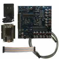
Manufacturer Part Number
CDB48500-USB
Description
KIT USB EVALUATION FOR CDB48500
Manufacturer
Cirrus Logic Inc
Datasheet
1.CDB48500-USB.pdf
(52 pages)
Specifications of CDB48500-USB
Main Purpose
Audio, Audio Processing
Embedded
No
Utilized Ic / Part
CS485XX
Primary Attributes
32-Bit Audio Processor, I2C or SPI
Secondary Attributes
Graphic User Interface, 12-ch Analog Audio Input & Outputs, Optical Out- S/PDIF
Description/function
Audio A/D
Operating Supply Voltage
9 V to 12 V
Product
Audio Modules
Supply Current
1 A
For Use With/related Products
CS48520, CS48540, CS48560
Lead Free Status / RoHS Status
Contains lead / RoHS non-compliant
Lead Free Status / RoHS Status
Lead free / RoHS Compliant, Contains lead / RoHS non-compliant
Other names
598-1284


CDB48500 System Block Descriptions
CDB485x00-USB Evaluation Kit Guide
3-7
3.1.11.2 Clock and Data Flow for S/PDIF Input
Figure 3-3
source, as described in
from the incoming S/PDIF stream is the MCLK for the system. The CS8416 also generates SCLK and
LRCLK for the DAI side of the DSP from the recovered MCLK.
On the output side, the CS485XX slaves to MCLK from CS8416 and masters SCLK and LRCLK for the
DAC side of the CS42448.
An example of this clocking scheme can be found in pcm.cpa.
DAI
CS485XX
CS8416
illustrates the S/PDIF clocking architecture used when any S/PDIF RX is used as an audio
XMTA SPDIF OUT
PLL
DAO
Figure 3-3. Simplified Clock and Data Flow for S/PDIF Input
Section 4.2.2, “Changing the Audio Input Source” on page
MUXED_DSP_LRCLK1
MUXED_DSP_SCLK1
S/PDIF Input
MUXED_MCLK
DSP_SCLK
DSP_LRCLK
DSP_DA0[3:0]
©
Copyright 2008 Cirrus Logic , Inc.
SPDIF
Input
SDIN
SDOUT
CS42448
CS42448
Use these jumper settings for the clocking
2x
mode and inputs shown in diagram.
2x
4-3). MCLK recovered
DS784DB1
Related parts for CDB48500-USB
Image
Part Number
Description
Manufacturer
Datasheet
Request
R

Part Number:
Description:
Development Kit
Manufacturer:
Cirrus Logic Inc
Datasheet:
Part Number:
Description:
Development Kit
Manufacturer:
Cirrus Logic Inc
Datasheet:


Part Number:
Description:
High-efficiency PFC + Fluorescent Lamp Driver Reference Design
Manufacturer:
Cirrus Logic Inc
Datasheet:
Part Number:
Description:
Development Kit
Manufacturer:
Cirrus Logic Inc
Datasheet:
Part Number:
Description:
Development Kit
Manufacturer:
Cirrus Logic Inc
Datasheet:

Part Number:
Description:
Development Kit
Manufacturer:
Cirrus Logic Inc
Datasheet:
Part Number:
Description:
Development Kit
Manufacturer:
Cirrus Logic Inc
Datasheet:
Part Number:
Description:
Development Kit
Manufacturer:
Cirrus Logic Inc
Datasheet:
Part Number:
Description:
Development Kit
Manufacturer:
Cirrus Logic Inc
Datasheet:

Part Number:
Description:
EVALUATION BOARD FOR CS8427
Manufacturer:
Cirrus Logic Inc
Datasheet:

Part Number:
Description:
BOARD EVAL FOR CS8416 RCVR
Manufacturer:
Cirrus Logic Inc
Datasheet:

Part Number:
Description:
EVALUATION BOARD FOR CS8420
Manufacturer:
Cirrus Logic Inc
Datasheet:

Part Number:
Description:
KIT DEVELOPMENT EP9315 ARM9
Manufacturer:
Cirrus Logic Inc
Datasheet:

Part Number:
Description:
KIT DEVELOPMENT EP9302 ARM9
Manufacturer:
Cirrus Logic Inc
Datasheet: