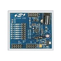
CP2120EK Silicon Laboratories Inc, CP2120EK Datasheet

CP2120EK
Specifications of CP2120EK
Related parts for CP2120EK
CP2120EK Summary of contents
Page 1
SPI Single Chip SPI Transfer Integrated clock; no external clock required On-Chip Voltage Monitor Slave Serial Peripheral Interface (SPI 1.0 Mbit/s ...
Page 2
CP2120 2 Rev. 0.4 ...
Page 3
ABLE F ONTENTS Section 1. System Overview . . . . . . . . . . . . . . . . . . . . . . . . . . . . . . ...
Page 4
CP2120 1. System Overview The CP2120 is a highly-integrated SPI-to-I reliable method for communicating with I 2 (SPI), a serial I C interface, 256 byte data buffers, an internal oscillator, eight input/output port pins, and one pin configurable as an ...
Page 5
Pinout And Package Definition 4.1. Pin Out Chart Name Pin # Type GND 2 RST 4 Digital I/O SCLK 1 Digital In MISO 20 Digital Out MOSI 19 Digital Digital In SDA 17 ...
Page 6
CP2120 4.2. QFN-20 Pinout Diagram (Top View 2120 ...
Page 7
QFN-20 Pinout Diagram (Bottom View) Table 4.1. QFN-20 Package Dimensions Rev. 0.4 CP2120 MM MIN TYP MAX 0.80 0.90 1.00 ...
Page 8
CP2120 4.4. QFN-20 Solder Paste Recommendations 8 Rev. 0.4 ...
Page 9
SPI Slave Bus The CP2120 provides a four-wire slave SPI interface. The CP2120's SPI Bus activates whenever the SPI Master pulls the NSS pin low. The master can then clock data into the CP2120 through the Master-Out-Slave-In (MOSI) pin ...
Page 10
CP2120 5.1. Command Set An SPI Master controls the CP2120 by sending commands across the SPI bus. Some commands initiate I transactions, while other commands modify or monitor CP2120 operation and events. 5.2. Internal Registers The CP2120 maintains a set ...
Page 11
Read From Internal Register COMMAND SPI Master 0x21 CP2120 A Read from Internal Register command retrieves the current value of one of the CP2120's internal registers. The command begins with the command byte, 0x21, followed by the internal register ...
Page 12
CP2120 Table 4. SPI Slave Timing Parameters * Slave Mode Timing (See Figure 4) T NSS Falling to First SCLK Edge SE T Last SCLK Edge to NSS Rising SD T NSS Falling to MISO Valid SEZ T NSS Rising ...
Page 13
I C Serial Interface 2 The CP2120 provides interface able to transfer data at frequencies up to 400 kHz. During a transaction, the 2 CP2120, operating as the I C master, sources a data clock ...
Page 14
CP2120 Internal Register Definition 1. I2CCLOCK: I R/W R/W I2CCK7 I2CCK6 I2CCK5 Bit 7 Bit 6 Internal Register Address: 0x02 Reset Value: 0xA0 Bit 7-0: I2CCK7-0: I maximum register value = 255) The transaction time-out counter, which terminates an I ...
Page 15
The SPI2I2C provides additional SMBus-related timers to enable I Free Detect enables the device to poll the SMBus lines and determine when a transfer can begin. Setting the SCL Low Time Out detect will cause an SMBus transaction to abort ...
Page 16
CP2120 Internal Register Definition 5. I2CSTAT I2ST7 I2ST6 I2ST5 Bit 7 Bit 6 Internal Register Address: 0x04 Reset Value: 0x00 Bit 7– Status Value 2 0xF0 I C transaction completed successfully. 0xF1 Slave address ...
Page 17
I C Receive Buffer Size 2 Bytes received from I C transactions are stored in the 255-byte data buffer. The number of bytes currently stored inside this buffer is saved in the RXBUFF Internal Register. Internal Register Definition ...
Page 18
CP2120 6.5.3. Read Buffer SPI Master CP2120 The Read Buffer command retrieves bytes from the CP2120's data buffer. The command begins with the command byte, 0x06. After the command byte, the SPI Master must transmit a single byte of data, ...
Page 19
Port I/O The CP2120 offers eight general-purpose port pins that can be configured as output, input, or quasi-bidirectional output by writing to the internal registers, IOCONFIG and IOCONFIG2. Pin state can be updated by writing to the internal register, ...
Page 20
CP2120 Internal Register Definition 8. IOCONFIG2: Port I/O Configuration 2 R/W R/W PCIO7.1 PCIO7.0 PCIO6.1 Bit 7 Bit 6 Internal Register Address: 0x07 Reset Value: 0x00 Bit 7-6: PCIO7.1-PCIO7.0: Port Configuration for GPIO Pin 7 Bit 5-4: PCIO6.1-PCIO6.0: Port Configuration ...
Page 21
Internal Register Definition 10. EDGEINT: Edge Triggered Interrupt Enable R/W R/W R/W EIF EIE EIT Bit 7 Bit 6 Bit 5 Internal Register Address: 0x08 Reset Value: 0x00 Bit 7: EIF: Edge Triggered Interrupt Flag 0: No edge triggered event ...
Page 22
CP2120 8. CP2120 Revision Number The CP2120 revision number can be retrieved by first sending the Revision Number command byte of 0x40 and then transmitting one “don’t care” transitional byte. The CP2120 then transmits the two-byte revision number, most significant ...
Page 23
OCUMENT HANGE IST Revision 0.1 to Revision 0.2 Various small text changes. Updated 4.1 Pin Out Chart. Updated 4.2 Pin Out Diagram. Updated Figure 2. SPI Bus Typical Connections. Added Table 3. ...
Page 24
... Should Buyer purchase or use Silicon Laboratories products for any such unintended or unauthorized application, Buyer shall indemnify and hold Silicon Laboratories harmless against all claims and damages. Silicon Laboratories, Silicon Labs, and USBXpress are trademarks of Silicon Laboratories Inc. Other products or brandnames mentioned herein are trademarks or registered trademarks of their respective holders 24 Rev ...


