EVAL-AD7674CBZ Analog Devices Inc, EVAL-AD7674CBZ Datasheet
EVAL-AD7674CBZ
Specifications of EVAL-AD7674CBZ


Related parts for EVAL-AD7674CBZ


EVAL-AD7674CBZ Summary of contents
Page 1
FEATURES 18-bit resolution with no missing codes No pipeline delay (SAR architecture) Differential input range: ± REF REF Throughput: 800 kSPS (Warp mode) 666 kSPS (Normal mode) 570 kSPS (Impulse mode) INL: ±2.5 LSB max ...
Page 2
... MAX Changes to Gain Error Parameter ........................... 3 MIN MAX Changes to Endnote 3 ...................................................................... 4 Changes to Pin Configuration Section .......................................... 8 Changes to Evaluating the AD7679’s Performance Section ...... 25 Changes to Ordering Guide .......................................................... 26 7/03—Revision 0: Initial Version Converter Operation .................................................................. 16 Typical Connection Diagram ................................................... 18 Power Dissipation versus Throughput .................................... 20 Conversion Control ................................................................... 20 Digital Interface .......................................................................... 20 Parallel Interface ...
Page 3
SPECIFICATIONS Table 2. –40°C to +85° 4.096 V, AVDD = DVDD = 5 V, OVDD = 2 5.25 V, unless otherwise noted. REF Parameter RESOLUTION ANALOG INPUT Voltage Range Operating Input Voltage Analog Input CMRR Input ...
Page 4
AD7674 Parameter REFERENCE External Reference Voltage Range REF Voltage with Reference Buffer Reference Buffer Input Voltage Range REFBUFIN Input Current REF Current Drain DIGITAL INPUTS Logic Levels DIGITAL OUTPUTS 5 Data Format ...
Page 5
TIMING SPECIFICATIONS Table 3. –40°C to +85°C, AVDD = DVDD = 5 V, OVDD = 2 5.25 V, unless otherwise noted. Parameter Refer to Figure 34 and Figure 35 Convert Pulsewidth Time between Conversions (Warp Mode/Normal Mode/Impulse Mode) ...
Page 6
AD7674 Table 4. Serial Clock Timings in Master Read after Convert DIVSCLK[1] DIVSCLK[0] SYNC to SCLK First Edge Delay Minimum Internal SCLK Period Minimum Internal SCLK Period Maximum Internal SCLK HIGH Minimum Internal SCLK LOW Minimum SDOUT Valid Setup Time ...
Page 7
ABSOLUTE MAXIMUM RATINGS Table 5. AD7674 Absolute Maximum Ratings Parameter Analog Inputs 2 2 IN+ , IN– , REF, REFBUFIN, REFGND to AGND Ground Voltage Differences AGND, DGND, OGND Supply Voltages AVDD, DVDD, OVDD AVDD to DVDD, AVDD to OVDD ...
Page 8
AD7674 PIN CONFIGURATION AND FUNCTION DESCRIPTIONS D4/DIVSCLK[0] D5/DIVSCLK[1] NOTES CONNECT. 2. THE EXPOSED PAD IS INTERNALLY CONNECTED TO AGND. THIS CONNECTION IS NOT REQUIRED TO MEET THE ELECTRICAL PERFORMANCES HOWEVER, FOR INCREASED RELIABILITY OF THE SOLDER ...
Page 9
Pin No. Mnemonic Type Description 9 D2/A1 DI/O When MODE = (18-bit or 16-bit interface mode), this pin is Bit 2 of the parallel port data output bus. In all other modes, this input pin controls ...
Page 10
AD7674 1 Pin No. Mnemonic Type Description 29 BUSY DO Busy Output. Transitions HIGH when a conversion is started. Remains HIGH until the conversion is complete and the data is latched into the on-chip shift register. The falling edge of ...
Page 11
DEFINITIONS OF SPECIFICATIONS Integral Nonlinearity Error (INL) Linearity error refers to the deviation of each individual code from a line drawn from negative full scale through positive full scale. The point used as negative full scale occurs ½ LSB before ...
Page 12
AD7674 TYPICAL PERFORMANCE CHARACTERISTICS 2.5 2.0 1.5 1.0 0.5 0 –0.5 –1.0 –1.5 0 65536 131072 CODE Figure 5. Integral Nonlinearity vs. Code 70000 59121 58556 60000 50000 40000 30000 20000 10000 5073 2004C 2004D 2004E ...
Page 13
POSITIVE DNL (LSB) Figure 11. Typical Positive DNL Distribution (424 Units – REF SNR = 98.4dB –40 THD = 119.1dB SFDR = 120.4dB ...
Page 14
AD7674 105 104 103 102 101 100 –60 –50 –40 –30 INPUT LEVEL (dB) Figure 17. SNR and S/(N+D) vs. Input Level 100 SNR 99 S/(N+ –55 –35 – ...
Page 15
POSITIVE 10 FULL SCALE 0 ZERO ERROR 10 20 NEGATIVE FULL SCALE –30 4.50 4.75 5.00 AVDD (V) Figure 23. Zero Error, Positive and Negative Full Scale vs. Supply 5.25 5.50 0 ...
Page 16
AD7674 CIRCUIT INFORMATION IN+ REF REFGND IN– The AD7674 is a very fast, low power, single-supply, precise 18-bit analog-to-digital converter (ADC) using successive approximation architecture. The AD7674’s linearity and dynamic range are similar to or better than many Σ-Δ ADCs. ...
Page 17
Transfer Functions Except in 18-bit interface mode, the AD7674 offers straight binary and twos complement output coding when using OB See Figure 26 and Table 8 for the ideal transfer characteristic. 111...111 111...110 111...101 000...010 000...001 000...000 –FS ...
Page 18
AD7674 TYPICAL CONNECTION DIAGRAM Figure 27 shows a typical connection diagram for the AD7674. Different circuitry shown on this diagram is optional and is discussed later in this data sheet. Analog Inputs Figure 28 shows a simplified analog input section ...
Page 19
SNR 20 log LOSS ⎜ ⎜ + π ⎜ 625 f ( ⎝ – 3dB where the –3 dB input bandwidth in MHz of the AD7674 –3dB (26 MHz) or the cutoff frequency ...
Page 20
AD7674 100 FREQUECY (kHz) Figure 32. PSRR vs. Frequency POWER DISSIPATION VERSUS THROUGHPUT In Impulse mode, the AD7674 automatically reduces its power consumption at the end of each conversion phase. During ...
Page 21
RESET BUSY DATA BUS CNVST Figure 35. RESET Timing CNVST t 10 BUSY t 3 DATA PREVIOUS CONVERSION DATA BUS Figure 36. Master Parallel Data Timing for Reading (Continuous Read) PARALLEL ...
Page 22
AD7674 In Read after Conversion mode, it should be noted that unlike in other modes, the BUSY signal returns low after the 18 data bits are pulsed out and not at the end of the conversion phase, which results in ...
Page 23
This is particularly important during the second half of the conversion phase because the AD7674 provides error correction circuitry that can correct for an improper bit decision made during the first half of ...
Page 24
AD7674 CS CNVST BUSY t 3 SCLK SDOUT t 16 Figure 43. Slave Serial Data Timing for Reading (Read Previous Conversion during Convert) BUSY AD7674 #2 (UPSTREAM) #1 (DOWNSTREAM) RDC/SDIN SDOUT RDC/SDIN CNVST CS SCLK SCLK CNVST ...
Page 25
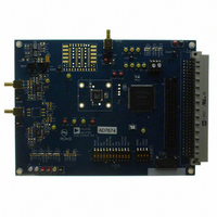
... An evaluation board for the AD7674 allows a quick means to measure both DC (histograms and time domain) and AC (time and frequency domain) performances of the converter. The EVAL-AD7674CBZ is an evaluation board package that includes a fully assembled and tested evaluation board, documentation, and software. The accompanying software ...
Page 26
... AD7674ASTZ −40°C to +85°C AD7674ASTZL −40°C to +85°C AD7674ACPZ −40°C to +85°C AD7674ACPZRL −40°C to +85°C 2 EVAL-AD7674CBZ EVAL-CED1Z 3 3 EVAL-CONTROL BRD2Z EVAL-CONTROL BRD3Z RoHS Compliant Part. 2 This board can be used as a standalone evaluation board or in conjunction with a capture board for evaluation/demonstration purposes. ...
Page 27
NOTES Rev Page AD7674 ...
Page 28
AD7674 NOTES ©2003–2009 Analog Devices, Inc. All rights reserved. Trademarks and registered trademarks are the property of their respective owners. D03083-0-6/09(A) Rev Page ...