DEMOTS4956J STMicroelectronics, DEMOTS4956J Datasheet
DEMOTS4956J
Specifications of DEMOTS4956J
DEMOTS4956J
Available stocks


Related parts for DEMOTS4956J


DEMOTS4956J Summary of contents
Page 1
Stereo audio amplifier system with I Features ■ Operating from ■ bus control interface ■ output power THD = 1 kHz, ...
Page 2
Contents Contents 1 Absolute maximum ratings and operating conditions . . . . . . . . . . . . . 4 2 Typical application schematic . . . . . . . . . . . . . ...
Page 3
TS4956 5 Package information . . . . . . . . . . . . . . . . . . . . . . . . . . . . . . . . . . . . ...
Page 4
Absolute maximum ratings and operating conditions 1 Absolute maximum ratings and operating conditions Table 1. Absolute maximum ratings Symbol V Supply voltage CC V Input voltage i T Operating free air temperature range oper T Storage temperature stg T Maximum ...
Page 5
TS4956 2 Typical application schematic Table 4. Description of external components Components Supply bypass capacitors which provide power supply filtering Bypass capacitor which provides half-supply filtering. b Input capacitors which form together with input ...
Page 6
Typical application schematic Figure 2. Typical application for the TS4956 (mode 7) SE input left Cin3 + 330nF SE input right Cin4 + 330nF 6/55 Vcc TS4956 Stereo MIP A1 Input Left Stereo MIN A2 Input Right Mode Select LIN ...
Page 7
TS4956 2 2 interface The TS4956 uses a serial bus, which conforms to the I powered when it is connected to the I clock and data. The clock and data lines are bidirectional (open-collector) with an external chip ...
Page 8
Typical application schematic In order to read data from the TS4956, after the "start" message, the MCU must send and receive the following data: ● send byte with the I²C 7-bit slave address and with the R/W bit set high. ...
Page 9
TS4956 2.1.2 Gain and mode setting operations The gain of the TS4956 ranges from -34 +12 dB. At power-up, the output channels are set to standby mode. Table 8. Gain settings truth table G: Gain (dB) # -34.5 ...
Page 10
Typical application schematic Table 9. Output mode settings truth table 2.1.3 Acknowledge bit The number of data bytes transferred between the start and the stop conditions from the CPU master to ...
Page 11
TS4956 3 Electrical characteristics Table 10 +2.7 V, GND = Symbol Parameter I Supply current CC I Standby current STBY V Output offset voltage OO Headphone output power (phantom ground mode) BTL, speaker output ...
Page 12
Electrical characteristics Table 10 +2.7 V, GND = Symbol Parameter Crosstalk Channel separation SNR Signal-to-noise ratio G Digital gain range Digital gain stepsize Stepsize error Input impedance, all gain Z in setting t Wake-up ...
Page 13
TS4956 Table 11 +3.3 V, GND = Symbol Parameter I Supply current CC I Standby current STBY V Output offset voltage OO Headphone output power (phantom ground mode) BTL, speaker output P out power ...
Page 14
Electrical characteristics Table 11 +3.3 V, GND = Symbol Parameter Crosstalk Channel separation SNR Signal-to-noise ratio G Digital gain range Digital gain stepsize Stepsize error Input impedance, all gain Z in setting t Wake-up ...
Page 15
TS4956 Table 12 GND = Symbol Parameter I Supply current CC I Standby current STBY V Output offset voltage OO Headphone output power (phantom ground mode) BTL, speaker output P out power ...
Page 16
Electrical characteristics Table 12 GND = Symbol Parameter Crosstalk Channel separation SNR Signal-to-noise ratio G Digital gain range Digital gain stepsize Stepsize error Input impedance, all gain Z in setting t Wake-up ...
Page 17
TS4956 Table 13. Output noise +12 dB A-weighted filter V (µV) out Mode 1 - SPK out 54 Mode 2 - SPK out 67 Mode 3 - LHP, RHP 55 Mode 4 - LHP, RHP 29 ...
Page 18
Electrical characteristics Figure 4. THD+N vs. output power 10 Mode SPK out Ω +1.5dB BW < 125kHz Vcc=3.3V ° Tamb = 25 C F=20kHz 1 Vcc=2.7V F=20kHz 0.1 Vcc=3.3V Vcc=2.7V F=1kHz ...
Page 19
TS4956 Figure 10. THD+N vs. output power 10 Mode 3 - LHP, RHP Ω +1.5dB BW < 125kHz ° Tamb = Vcc=2.7V F=20kHz 0.1 Vcc=3.3V Vcc=5V Vcc=2.7V F=20kHz F=20kHz F=1kHz 0.01 ...
Page 20
Electrical characteristics Figure 16. THD+N vs. output power 10 Mode MLO Ω +1.5dB BW < 125kHz ° Tamb = Vcc=2.7V F=20kHz 0.1 Vcc=2.7V Vcc=3.3V F=1kHz F=1kHz 0.01 1E-3 ...
Page 21
TS4956 Figure 22. THD+N vs. frequency 10 Mode SPK out Ω +1.5dB BW < 125kHz ° Tamb = Vcc=3.3V Vcc=2.7V Po=300mW Po=200mW 0.1 0.01 20 100 Frequency (Hz) Figure ...
Page 22
Electrical characteristics Figure 28. THD+N vs. frequency 10 Mode 3 - LHP, RHP Ω +1.5dB BW < 125kHz ° Tamb = Vcc=2.7V Po=10mW 0.1 0.01 20 100 Frequency (Hz) Figure 30. THD+N ...
Page 23
TS4956 Figure 34. THD+N vs. frequency 10 Mode MLO Ω +1.5dB BW < 125kHz ° Tamb = Vcc=3.3V Vcc=2.7V Po=50mW Po=30mW 0.1 0.01 20 100 Frequency (Hz) Figure 36. ...
Page 24
TS4956 Figure 40. Output power vs. power supply voltage 1400 Mode 1300 BTL, SPK out 1200 F = 1kHz 1100 BW < 125 kHz 1000 ° Tamb = 25 C 900 800 Ω RL=16 700 600 500 ...
Page 25
TS4956 Figure 46. Output power vs. load resistance 1400 1300 1200 Vcc=5.5V 1100 1000 900 Vcc=5V 800 700 600 Vcc=3.3V 500 400 Vcc=2.7V 300 200 100 Load resistance ( Figure 48. Output power vs. load ...
Page 26
TS4956 Figure 52. PSRR vs. frequency 0 Mode 1 - SPK out Vcc = 2.7V ≥ Ω μ - Inp. grounded Vripple = 200mVpp -40 G=+6dB -60 -80 G=-34.5dB -100 20 100 Frequency ...
Page 27
TS4956 Figure 58. PSRR vs. frequency 0 Mode 3 - LHP, RHP -10 Vcc = 2.7V ≥ Ω , μ -20 Inp. grounded -30 Vripple = 200mVpp -40 G=+1.5dB G=+6dB -50 -60 -70 -80 ...
Page 28
TS4956 Figure 64. PSRR vs. frequency 0 Mode 5 - MLO -10 Vcc = 2.7V ≥ Ω , μ - Inp. grounded G=+12dB -30 Vripple = 200mVpp -40 -50 -60 -70 -80 G=-9dB -90 ...
Page 29
TS4956 Figure 70. PSRR vs. frequency 0 Mode 7 - BTL, SPK out -10 Vcc = 2.7V ≥ Ω , μ -20 Inp. grounded -30 Vripple = 200mVpp G=+12dB -40 -50 G=+1.5dB -60 -70 ...
Page 30
TS4956 Figure 76. SNR vs. power supply voltage 100 Weighted filter type Unweighted filter (20Hz to 20 kHz) 72 Mode 1, SPK out 70 Ω G ...
Page 31
TS4956 Figure 82. SNR vs. power supply voltage 100 Weighted filter type Unweighted filter (20Hz to 20kHz) 72 Mode 2, SPK out 70 Ω ...
Page 32
TS4956 Figure 88. SNR vs. power supply voltage 100 Weighted filter type A 74 Unweighted filter (20Hz to 20kHz) 72 Mode 4 - LHP, RHP 70 Ω G ...
Page 33
TS4956 Figure 94. SNR vs. power supply voltage 100 Weighted filter type Unweighted filter (20Hz to 20kHz) 72 Mode 5 - MLO 70 Ω ...
Page 34
TS4956 Figure 100. SNR vs. power supply voltage 100 Weighted filter type Unweighted filter (20Hz to 20kHz) 72 Mode 7 - BTL, SPKout 70 Ω G ...
Page 35
TS4956 Figure 106. Frequency response modes G=+12dB, RL=32 8 Ω G=+12dB, RL= G=+6dB, RL=32 -2 G=+6dB, RL=16 -4 Ω G=+1.5dB, RL=32 -6 Ω G=+1.5dB, RL=16 -8 -10 100 Frequency (Hz) Figure 108. ...
Page 36
TS4956 Figure 112. Power dissipation vs. output power (per channel) 90 THD+N= Output Power (mW) Figure 114. Power dissipation vs. output power (per channel) 130 120 THD+N=1% 110 ...
Page 37
TS4956 Figure 118. Power dissipation vs. output power Figure 119. Power dissipation vs. output power THD+N=1% 50 RL= Ω RL= 100 120 140 160 180 200 ...
Page 38
TS4956 4 Application information The TS4956 integrates four monolithic power amplifiers and has one differential input and two single-ended inputs. The output amplifiers can be configured in 7 different modes as one SE (single-ended) capacitively-coupled output, two phantom ground headphone ...
Page 39
TS4956 4.1.4 BTL output configuration (modes BTL (bridge tied load) output configuration (modes 1, 2 and 4), active outputs are biased to the V CC except for the MLO output, which is biased to V ...
Page 40
TS4956 4.3 Power dissipation and efficiency Hypotheses: ● The voltage and current in the load are sinusoidal (V ● The supply voltage is a pure DC source (V Regarding the load we have: and and 4.3.1 Single-ended output configuration (modes ...
Page 41
TS4956 and its value is: Note: This maximum value depends only on the power supply voltage and load values. The efficiency is the ratio between the output power and the power supply: The maximum theoretical value is reached when V ...
Page 42
TS4956 The efficiency is the ratio between the output power and the power supply. The maximum theoretical value is reached when V In modes 3 and 4, the TS4956 has two active output power amplifiers. Each amplifier produces heat due ...
Page 43
TS4956 and the maximum value is obtained when: and its value is: Note: This maximum value depends only on the power supply voltage and load values. The efficiency is the ratio between the output power and the power supply. The ...
Page 44
TS4956 4.4 Low frequency response 4.4.1 Input capacitor C The input coupling capacitor blocks the DC part of the input signal at the amplifier input. In the low-frequency region, C pass filter with -3 dB cut-off frequency the ...
Page 45
TS4956 Figure 128. 3dB lower cut off frequency vs. output capacitance 4.5 Single-ended input configuration in modes 1, 3 and possible to use the differential inputs MIP and MIN of the TS4956 as one single-ended input in ...
Page 46
TS4956 4.6 Decoupling of the circuit Two capacitors are needed to properly bypass the TS4956 — a power supply capacitor C and a bias voltage bypass capacitor C C has a strong influence on the THD+N at high frequencies (above ...
Page 47
TS4956 4.8 PSRR measurements 4.8.1 What is PSRR? The PSRR is the power supply rejection ratio. The PSRR of a device is the ratio between a power supply disturbance and the result on the output. In other words, the PSRR ...
Page 48
TS4956 4.9 Pop and click performance The TS4956 has an internal pop and click reduction circuitry which eliminates the output transients, such as, for example, during switch-on or switch-off phases, or during a switch from one output mode to another, ...
Page 49
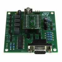
TS4956 4.11 Demonstration board A demonstration board for the TS4956 is available. For more information about this demonstration board, refer to the application note AN2465, which you can find on www.st.com. Figure 131. Demonstration board schematic for the TS4956 Diff. ...
Page 50
TS4956 5 Package information In order to meet environmental requirements, ST offers these devices in different grades of ® ECOPACK packages, depending on their level of environmental compliance. ECOPACK specifications, grade definitions and product status are available at: www.st.com. ® ...
Page 51
TS4956 Figure 134. Pinout (top view PGH PGH PGH PGH PGH GND GND GND GND GND LHP- LHP- RHP RHP RHP LHP ...
Page 52
TS4956 5.2 Daisy chain sample The daisy chain sample features pins connected two by two. in which the pins are connected to each other. This sample is used for testing continuity on the board. The PCB needs to be designed ...
Page 53
TS4956 6 Ordering information Table 14. Order code for daisy chain sample Order code Temperature range TSDC02JT -40, +85° C Table 15. Order codes Order code Temperature range TS4956EIJT -40°C to +85°C Package Flip-Chip18 Package Packing Lead free flip-chip18 Tape ...
Page 54
TS4956 7 Revision history Table 16. Document revision history Date 01-Nov-2005 01-Dec-2005 01-May-2006 10-Mar-2009 Revision 1 First release corresponding to the preliminary data version. 2 Cancellation of the back coating sale type. 3 Final datasheet. Document reformatted. 4 Updated input ...
Page 55
... TS4956 Information in this document is provided solely in connection with ST products. STMicroelectronics NV and its subsidiaries (“ST”) reserve the right to make changes, corrections, modifications or improvements, to this document, and the products and services described herein at any time, without notice. All ST products are sold pursuant to ST’s terms and conditions of sale. ...