STEVAL-ISA034V1 STMicroelectronics, STEVAL-ISA034V1 Datasheet
STEVAL-ISA034V1
Specifications of STEVAL-ISA034V1
STEVAL-ISA034V1


Related parts for STEVAL-ISA034V1


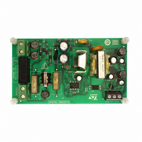
STEVAL-ISA034V1 Summary of contents
Page 1
... Application Switching applications Description Using the well consolidated high voltage MESH TM OVERLAY process, STMicroelectronics has designed an advanced family of very high voltage Power MOSFETs with outstanding performances. The strengthened layout coupled with the company’s proprietary edge termination structure, gives the lowest R ...
Page 2
Contents Contents 1 Electrical ratings . . . . . . . . . . . . . . . . . . . . . . . . . . . . . . . . . . . ...
Page 3
STFW3N150, STP3N150, STW3N150 1 Electrical ratings Table 2. Absolute maximum ratings Symbol V Drain-source voltage ( Gate-source voltage GS I Drain current (continuous Drain current (continuous (1) I Drain current (pulsed) ...
Page 4
Electrical characteristics 2 Electrical characteristics ( °C unless otherwise specified) case Table 5. On /off states Symbol Drain-source V (BR)DSS breakdown voltage Zero gate voltage I DSS drain current (V Gate-body leakage I GSS current (V V Gate ...
Page 5
STFW3N150, STP3N150, STW3N150 Table 7. Switching times Symbol t Turn-on delay time d(on) t Rise time r t Turn-off-delay time d(off) t Fall time f Table 8. Source drain diode Symbol I Source-drain current SD (1) I Source-drain current (pulsed) ...
Page 6
Electrical characteristics 2.1 Electrical characteristics (curves) Figure 2. Safe operating area for TO-3PF Tj=150°C 0.1 Tc=25°C Sinlge pulse 0.01 10 0.1 1 100 Figure 4. Safe operating area for TO-220 Figure 6. Safe operating area ...
Page 7
STFW3N150, STP3N150, STW3N150 Figure 8. Output characteristics Figure 10. Normalized BV DSS Figure 12. Gate charge vs. gate-source voltage Figure 9. vs. temperature Figure 11. Static drain-source on resistance Figure 13. Capacitance variations Doc ID 13102 Rev 9 Electrical characteristics ...
Page 8
Electrical characteristics Figure 14. Normalized gate threshold voltage vs. temperature Figure 16. Source-drain diode forward characteristics 8/15 STFW3N150, STP3N150, STW3N150 Figure 15. Normalized on resistance vs. temperature Figure 17. Maximum avalanche energy vs Tj Doc ID 13102 Rev 9 ...
Page 9
STFW3N150, STP3N150, STW3N150 3 Test circuits Figure 18. Switching times test circuit for resistive load D.U. Figure 20. Test circuit for inductive load switching and diode recovery times A A ...
Page 10
Package mechanical data 4 Package mechanical data In order to meet environmental requirements, ST offers these devices in different grades of ® ECOPACK packages, depending on their level of environmental compliance. ECOPACK specifications, grade definitions and product status are available ...
Page 11
STFW3N150, STP3N150, STW3N150 Dim L20 L30 ∅P Q TO-220 mechanical data mm Min Typ Max 4.40 4.60 0.61 0.88 1.14 1.70 0.48 0.70 15.25 15.75 1.27 ...
Page 12
Package mechanical data Dim øP øR S 12/15 TO-247 Mechanical data mm. Min. Typ 4.85 2.20 1.0 2.0 3.0 0.40 19.85 15.45 5.45 14.20 3.70 18.50 3.55 4.50 ...
Page 13
STFW3N150, STP3N150, STW3N150 DIM Dia TO-3PF mechanical data mm. min. typ 5.30 2.80 3.10 1.80 0.80 0.65 1.80 10.30 5.45 15.30 ...
Page 14
Revision history 5 Revision history Table 9. Document revision history Date 12-Jan-2007 17-Apr-2007 14-May-2007 29-Aug-2007 09-Apr-2008 13-Feb-2009 01-Dec-2009 10-Dec-2009 29-Jun-2010 14/15 Revision 1 First release 2 Added new value on 3 The document has been reformatted 4 R value changed, ...
Page 15
... STFW3N150, STP3N150, STW3N150 Information in this document is provided solely in connection with ST products. STMicroelectronics NV and its subsidiaries (“ST”) reserve the right to make changes, corrections, modifications or improvements, to this document, and the products and services described herein at any time, without notice. All ST products are sold pursuant to ST’s terms and conditions of sale. ...