EVL250W-ATX80PL STMicroelectronics, EVL250W-ATX80PL Datasheet - Page 6
EVL250W-ATX80PL
Manufacturer Part Number
EVL250W-ATX80PL
Description
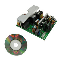
BOARD DEMO SMPS L6591/L6563S
Manufacturer
STMicroelectronics
Series
VIPer™ plusr
Datasheet
1.EVL250W-ATX80PL.pdf
(45 pages)
Specifications of EVL250W-ATX80PL
Main Purpose
Power Supply, ATX
Outputs And Type
3, Isolated
Power - Output
250W
Voltage - Output
12V, 5V, 3.3V
Current - Output
13.5A, 12A, 8A
Voltage - Input
88 ~ 264VAC
Regulator Topology
Flyback
Frequency - Switching
80kHz
Board Type
Fully Populated
Utilized Ic / Part
L6563S, L6591, L6727, VIPer27H
Input Voltage
88 VAC to 264 VAC
Output Voltage
3.3 V, 5 V, 12 V
Maximum Operating Temperature
+ 60 C
Operating Supply Voltage
80 VAC to 264 VAC
Output Power
250 W
Product
Power Management Development Tools
Lead Free Status / RoHS Status
Lead free / RoHS Compliant
For Use With/related Products
L6563S PFC controller
Other names
497-10596


Main characteristics and circuit description
6/45
and protection needed by the AHB stage and an interface for the PFC controller. The L6591
includes two gate drivers for the half bridge MOSFETs and a fixed frequency
complementary PWM logic with 50 % maximum duty cycle with programmable dead time
and current mode control technique.
Other features of this IC are pulse-by-pulse overcurrent protection, transformer saturation
detection, overload protection (latched or auto-restart), and programmable soft-start. There
is also a high voltage startup circuit, a burst mode logic for low load operation, and the
adaptive UVLO onboard, which are not used in this design as they are designed for adapter
applications (see AN2852).
The following is a description of the power circuit of this stage. The half bridge switches
Q101 and Q102 are connected to the output voltage of the PFC. The half bridge node drives
the series of C101 (DC blocking capacitor) and the primary side of the transformer T1. This
transformer has two secondary windings with a center tap connected to the secondary
ground. The other ends are connected to the sources of MOSFETs Q201 and Q202, which
replace output diodes in order to perform the synchronous rectification. Two extra windings
allow, with few external passive components, a self driven synchronous rectification to be
obtained. This solution allows efficiency to be increased without the extra cost of a
dedicated SR controller IC.
Q201 and Q202 drains are connected to the output inductor L201 that, together with output
capacitors C201 and C202, acts as a low pass filter. The signal +12 VA is then post filtered
(with L5 and C207) to obtain the +12 V output voltage.
The design of transformer T1 is a trade-off between ZVS operation and the required
electrical performance/efficiency. ZVS can be obtained acting on the magnetizing
inductance or on the primary side leakage inductance. In more detail, ZVS could be met by:
●
●
Low values of magnetizing inductance generate high magnetizing current. This helps to
reach ZVS but it also increases the total primary side rms current and therefore the related
losses. In this design a value of 500 µH has been selected.
On the other hand, ZVS could be obtained by increasing the leakage inductance. If such a
parameter is increased, the primary side current takes more time before reversing its
direction and therefore ZVS is more easily met. A high leakage inductance value leads to
duty cycle losses, reducing the effective range of duty cycle usable. This creates problems
with hold-up requirements and makes it necessary to work with very narrow duty cycles with
nominal input voltage generating high rms currents in the circuit.
A value of 12 µH has been selected as the leakage inductance.
Because of these reasons, in this design ZVS is always met at low side MOSFET turn-on
while it is met only for medium-high loads at high side MOSFET turn-on. Even at medium-
low loads Q101 is turned on with a Vds well below the half bridge input voltage.
The L6591 LINE pin is used for startup sequencing. It shares with the L6563S the voltage
divider made up of R20, R21, R22, R29, and R26 that senses the PFC output voltage. The
AHB stage is activated when the bulk voltage reaches about 380 V.
The DISABLE pin (latched protection) is driven by the L6563S PWM_LATCH pin and stops
the AHB stage in case of PFC feedback disconnection.
The oscillator is programmed in order to have a switching frequency of about 80 KHz and to
use the minimum dead time (about 310 ns).
Decreasing the magnetizing inductance
Increasing the leakage inductance
Doc ID 17402 Rev 1
AN3203
Related parts for EVL250W-ATX80PL
Image
Part Number
Description
Manufacturer
Datasheet
Request
R

Part Number:
Description:
STMicroelectronics [RIPPLE-CARRY BINARY COUNTER/DIVIDERS]
Manufacturer:
STMicroelectronics
Datasheet:
Part Number:
Description:
STMicroelectronics [LIQUID-CRYSTAL DISPLAY DRIVERS]
Manufacturer:
STMicroelectronics
Datasheet:

Part Number:
Description:
BOARD EVAL FOR MEMS SENSORS
Manufacturer:
STMicroelectronics
Datasheet:
Part Number:
Description:
NPN TRANSISTOR POWER MODULE
Manufacturer:
STMicroelectronics
Datasheet:
Part Number:
Description:
TURBOSWITCH ULTRA-FAST HIGH VOLTAGE DIODE
Manufacturer:
STMicroelectronics
Datasheet:
Part Number:
Description:
Manufacturer:
STMicroelectronics
Datasheet:
Part Number:
Description:
DIODE / SCR MODULE
Manufacturer:
STMicroelectronics
Datasheet:
Part Number:
Description:
DIODE / SCR MODULE
Manufacturer:
STMicroelectronics
Datasheet:
Part Number:
Description:
Search -----> STE16N100
Manufacturer:
STMicroelectronics
Datasheet:
Part Number:
Description:
Search ---> STE53NA50
Manufacturer:
STMicroelectronics
Datasheet:
Part Number:
Description:
NPN Transistor Power Module
Manufacturer:
STMicroelectronics
Datasheet:
Part Number:
Description:
DIODE / SCR MODULE
Manufacturer:
STMicroelectronics
Datasheet: