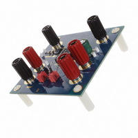
ISL8201MEVAL1Z Intersil, ISL8201MEVAL1Z Datasheet

ISL8201MEVAL1Z
Specifications of ISL8201MEVAL1Z
Related parts for ISL8201MEVAL1Z
ISL8201MEVAL1Z Summary of contents
Page 1
... CAUTION: These devices are sensitive to electrostatic discharge; follow proper IC Handling Procedures. | 1-888-INTERSIL or 1-888-468-3774 Intersil (and design registered trademark of Intersil Americas Inc. Copyright Intersil Americas Inc. 2009, 2010. All Rights Reserved All other trademarks mentioned are the property of their respective owners. ISL8201M FN6657 ...
Page 2
... PART NUMBER (Notes ISL8201MIRZ ISL8201MEVAL1Z 1. Add “-T” suffix for tape and reel. Please refer to 2. These Intersil plastic packaged products employ special material sets, molding compounds and 100% matte tin plate plus anneal (e3) termination finish. These products do contain Pb but they are RoHS compliant by EU exemption 5 (Pb in glass of cathode ray tubes, electronic components and fluorescent tubes) ...
Page 3
Pinout Pin Descriptions PIN SYMBOL PGND 5 PVCC ISET 9 VIN 10 PHASE 12 VOUT 13 COMP/ ISL8201M ISL8201M (15 ...
Page 4
... Ld QFN (Notes GND VCC - 0.3V to +15V Junction Temperature T GND Storage Temperature Range T Pb-Free Reflow Profile .see link below http://www.intersil.com/pbfree/Pb-FreeReflow.asp Recommended Operating Ratings Input Supply Voltage (V Output Voltage (V P VCC Fixed Supply Voltage . . . . . . . . . . . . . . . . . . . . . . . . +5V or +12V Wide Range Supply . . . . . . . . . . . . . . . . . . . . . . +6.5V to +14.4V ...
Page 5
Electrical Specifications T = +25° 22µF/Ceramicx3. (Continued) PARAMETER Oscillator Frequency Internal Resistor Between V and FB Pins OUT Disabled Threshold Voltage (COMP/EN) Reference Voltage Reference Voltage Tolerance FAULT PROTECTION Internal Resistor Between I and P Pins SET GND ...
Page 6
Typical Performance Characteristics Transient Response Performance V = 12V 1.5V OUT OUT FIGURE 6. 1.5V TRANSIENT RESPONSE V = 12V 2.5V OUT OUT FIGURE ...
Page 7
Pin Functions PGND (Pins 11) Power ground pin for signal, input, and output return path. PGND needs to connect to one (or more) ground plane(s) immediately, which is recommended to minimize the effect of switching noise, ...
Page 8
Applications Information The typical ISL8201M application schematic for input voltage +5V or +12V is shown in Figure 11. External component selection is primarily determined by the maximum load current and input/output voltage. Programming the Output Voltage The ISL8201M has an ...
Page 9
ISET FIGURE 15. I AND SOFT-START OPERATION SET Soft-Start and Pre-Biased Outputs The soft-start internally ramps the reference on the non-inverting terminal of the error amp from nominal 6.8ms. The output voltage will thus follow ...
Page 10
VOUT 500mV/ diV FIGURE 18. PRE-BIASED START-UP - OVERCHARGED If the V for the synchronous buck converter is from a IN different supply that comes up after P go through its cycle, but with no output voltage ramp. When V ...
Page 11
The maximum r at the highest junction DS(ON) temperature 2. The minimum I from the “Electrical Specifications” SET table on page 3. 3. Determine I for: PEAK ( Δ > ------------- + ( ) PEAK ...
Page 12
This prevents a disturbance on the output, due to the internal regulator turning on or off. If the transition is slow (not a step change), the disturbance should be minimal. Thus, while the recommendation is to ...
Page 13
The ground connection between pin 11 and pin should be a solid ground plane under the module. • Place a high frequency ceramic capacitor between (1) VIN and PGND (pin 11) and (2) PVCC and PGND ...
Page 14
... Accordingly, the reader is cautioned to verify that data sheets are current before placing orders. Information furnished by Intersil is believed to be accurate and reliable. However, no responsibility is assumed by Intersil or its subsidiaries for its use; nor for any infringements of patents or other rights of third parties which may result from its use ...
Page 15
Package Outline Drawing L15.15x15 15 LEAD QUAD FLAT NO-LEAD PLASTIC PACKAGE (PUNCH QFN) Rev 3, 8/10 PIN 1 1 1514 13 12 INDEX AREA 15.0±0.2 15.8±0.2 TOP VIEW 5° ALL AROUND ...
Page 16
Package Boundary 3.00 2.20 1.70 0.90 0.40 0.0 0.0 0.40 0.90 1.70 2.20 3.00 4.00 8.30 TYPICAL RECOMMENDED LAND PATTERN 6.60 4.80 3.40 1.80 0.00 0.60 1.20 2.20 3.70 4.30 6.60 STENCIL PATTERN WITH ...


