CDB4398 Cirrus Logic Inc, CDB4398 Datasheet
CDB4398
Specifications of CDB4398


Related parts for CDB4398


CDB4398 Summary of contents
Page 1
Multi-Bit DAC with Volume Control Features Advanced Multi-bit Delta-Sigma Architecture – 120 dB Dynamic Range – -107 dB THD+N – Low Clock Jitter Sensitivity – Differential Analog Outputs PCM input – 102 dB of Stopband Attenuation ...
Page 2
... DSD audio data, has selectable dig- ital filters, consumes little power, and delivers excellent sound quality. Package Pb-Free Grade 28-pin YES Commercial TSSOP - - CS4398 Temp Range Container Order # Rail CS4398-CZZ -10° to +70° C Tape & Reel CS4398-CZZR - - CDB4398 DS568F1 ...
Page 3
TABLE OF CONTENTS 1. PINOUT DRAWING ................................................................................................................. 6 2. CHARACTERISTICS AND SPECIFICATIONS ........................................................................ 8 SPECIFIED OPERATING CONDITIONS ................................................................................. 8 ABSOLUTE MAXIMUM RATINGS ........................................................................................... 8 ANALOG CHARACTERISTICS................................................................................................ 9 COMBINED INTERPOLATION & ON-CHIP ANALOG FILTER RESPONSE ........................ 10 COMBINED INTERPOLATION & ON-CHIP ...
Page 4
LIST OF FIGURES Figure 1. Pinout Drawing................................................................................................................. 6 Figure 2. Serial Mode Input Timing ............................................................................................... 12 Figure 3. Format 0 - Left-Justified up to 24-bit Data ..................................................................... 13 Figure 4. Format 1 - I² 24-bit Data ..................................................................................... 13 ...
Page 5
LIST OF TABLES Table 1. Clock Ratios .................................................................................................................... 21 Table 2. Common Clock Frequencies........................................................................................... 22 Table 3. Digital Interface Format, Stand-Alone Mode Options...................................................... 22 Table 4. Mode Selection, Stand-Alone Mode Options .................................................................. 22 Table 5. Digital Interface Formats - PCM ...
Page 6
PINOUT DRAWING DSD_B DSD_SCLK SDIN SCLK LRCK MCLK VD DGND M3 (AD1/CDIN) M2 (SCL/CCLK) M1 (SDA/CDOUT) M0 (AD0/CS) RST VLC ...
Page 7
Pin Name Pin # DSD_A 28 Direct Stream Digital Input (Input) - Input for Direct Stream Digital serial audio data. DSD_B 1 DSD_SCLK 2 DSD Serial Clock (Input) - Serial clock for the Direct Stream Digital audio interface. SDIN 3 ...
Page 8
CHARACTERISTICS AND SPECIFICATIONS (Min/Max performance characteristics and specifications are guaranteed over the Specified Operating Conditions. Typical performance characteristics are derived from measurements taken at T SPECIFIED OPERATING CONDITIONS (AGND = 0 V; all voltages with respect to ground.) Parameters ...
Page 9
ANALOG CHARACTERISTICS (Test conditions (unless otherwise specified): Input test signal is a 997 Hz sine wave at 0 dBFS; measurement bandwidth kHz; test load R Parameter Dynamic Performance - All PCM modes and DSD Processor ...
Page 10
COMBINED INTERPOLATION & ON-CHIP ANALOG FILTER RESPONSE The filter characteristics have been normalized to the sample rate (Fs) and can be referenced to the desired sam- ple rate by multiplying the given characteristic by Fs.) (See note 9.) Parameter Combined ...
Page 11
COMBINED INTERPOLATION & ON-CHIP ANALOG FILTER RESPONSE (Continued) Parameter Single-Speed Mode - 48 kHz (Note 5) Passband (Note 6) Frequency Response kHz StopBand StopBand Attenuation Group Delay De-emphasis Error (Note 8) (Relative to 1 kHz) Double-Speed ...
Page 12
SWITCHING CHARACTERISTICS (Inputs: Logic 0 = GND, Logic 1 = VLS pF) Parameters Input Sample Rate Double-Speed Mode MCLK Frequency MCLK Duty Cycle LRCK Duty Cycle SCLK Pulse Width Low SCLK Pulse Width High SCLK Period Double-Speed ...
Page 13
Left C ha nnel Figure 3. Format 0 - Left-Justified up to 24-bit Data Left C ha nnel LR ...
Page 14
SWITCHING CHARACTERISTICS - DSD (Logic 0 = AGND = DGND; Logic 1 = VLS Volts; C Parameter MCLK Duty Cycle DSD_SCLK Pulse Width Low DSD_SCLK Pulse Width High DSD_SCLK Frequency DSD_A / _B valid to DSD_SCLK rising setup time DSD_SCLK ...
Page 15
SWITCHING CHARACTERISTICS - CONTROL PORT - I²C FORMAT (Inputs: Logic 0 = GND, Logic 1 = VLC, C Parameter SCL Clock Frequency RST Rising Edge to Start Bus Free-Time Between Transmissions Start Condition Hold Time (prior to first clock pulse) ...
Page 16
SWITCHING CHARACTERISTICS - CONTROL PORT - SPI (Inputs: Logic 0 = GND, Logic 1 = VLC, C Parameter CCLK Clock Frequency RST Rising Edge to CS Falling CCLK Edge to CS Falling CS High Time Between Transmissions CS Falling to ...
Page 17
DC ELECTRICAL CHARACTERISTICS Parameters Normal Operation (Note 16) Power Supply Current Power Dissipation Power-Down Mode (Note 19) Power Supply Current Power Dissipation All Modes of Operation Power Supply Rejection Ratio (Note 20) Common Mode Voltage Max Current draw from VQ ...
Page 18
DIGITAL INTERFACE SPECIFICATIONS Parameters Input Leakage Current Input Capacitance High-Level Input Voltage Low-Level Input Voltage High-Level Output Voltage (I = -1.2 mA) OH Low-Level Output Voltage (I = 1.2 mA) OL MUTEC auto detect input high voltage MUTEC auto detect ...
Page 19
TYPICAL CONNECTION DIAGRAM +3. 0.1 uF System Clock PCM Digital Audio Source +1.8V to 0.1 uF +5V DSD Audio Source +1.8V to 0.1 uF +5V µ Controler or stand alone pull-ups/ downs DS568F1 VD MCLK ...
Page 20
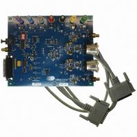
... The Cirrus Logic application note “Design Notes for a 2-Pole Filter with Differential Input” (AN48) discusses the second-order Butterworth filter and differential to single-ended converter topology that was implemented on the CS4398 evaluation board, CDB4398, as seen in Figure 11. The CS4398 does not include phase or amplitude compensation for an external filter. Therefore, the DAC system phase and amplitude response is dependent on the external analog circuitry ...
Page 21
Use of the Mute Control function is not mandatory but recommended for designs requiring the absolute min- imum in extraneous clicks and pops. Also, use of the Mute Control function can enable the system designer to achieve idle channel noise/signal-to-noise ...
Page 22
Mode Sample (sample- Rate rate range) (kHz) MCLK Ratio 32 Single-Speed ( kHz) 44.1 48 MCLK Ratio 64 Double-Speed (50 to 100 kHz) 88.2 96 MCLK Ratio 176.4 Quad-Speed (100 to 200 kHz) 192 12.2880* These modes are ...
Page 23
Recommended Power-up Sequence (Stand-Alone Mode) 1. Hold RST low until the power supply, master, and left/right clocks are stable. In this state, the Control Port is reset to its default settings. 2. Bring RST high. The device will remain ...
Page 24
Direct Stream Digital (DSD) Mode (Control Port Mode) In Control Port mode, the FM bits (Reg. 02h) are used to configure the device for DSD mode. The DIF bits (Reg 02h) then control the expected DSD rate and MCLK ...
Page 25
CONTROL PORT INTERFACE The Control Port is used to load all the internal settings. The operation of the Control Port may be completely asyn- chronous with the audio sample rate. However, to avoid potential interference problems, the Control Port ...
Page 26
Writing in I²C Format To communicate with the CS4398, initiate a START condition of the bus (see Figure 14.). Next, send the chip address. The eighth bit of the address byte is the R/W bit (low for a write). ...
Page 27
CS CCLK CHIP ADDRESS CDIN Figure 15. Control Port Timing, SPI Format (Write) 5.5.2 Reading in SPI Figure 16 shows the operation of the Control Port in SPI format. To read to a ...
Page 28
REGISTER QUICK REFERENCE Addr Function 7 1h Chip ID PART4 default 0 2h Mode Control DSD_SRC default 0 3h Volume, Mixing, VOLB=A and Inversion Control default 0 4h Mute Control PAMUTE default 1 5h Channel A Vol- VOL7 ume ...
Page 29
REGISTER DESCRIPTION ** All register access is R/W unless specified otherwise** 7.1 Chip ID - Register 01h 7 6 PART4 PART3 PART2 0 1 Function: This register is Read-Only. Bits 7 through 3 are the part number ID, which ...
Page 30
DSD Mode: The relationship between the oversampling ratio of the DSD audio data and the required Master Clock to DSD data rate is defined by the Digital Interface Format pins. DIF2 DIF1 DIF0 ...
Page 31
Channel B Volume = Channel A Volume (VOLB=A) Bit 7 Function: When set to 0 (default), the AOUTA and AOUTB volume levels are independently controlled by the A and the B Channel Volume Control Bytes. When set to 1, ...
Page 32
ATAPI4 ATAPI3 ATAPI2 ...
Page 33
Mute Control - Register 04h 7 6 PAMUTE DAMUTE MUTEC A 7.4.1 PCM Auto-mute (PAMUTE) Bit 7 Function: When set to 1 (default), the Digital-to-Analog converter output will mute following the reception of 8192 consecutive audio samples ...
Page 34
MUTE Polarity and DETECT (MUTEP1:0) Bits 1-0 Default = Auto polarity detect, selected from AMUTEC pin 01 - Reserved 10 - Active low mute polarity 11 - Active high mute polarity Function: Auto mute polarity detect ...
Page 35
Ramp and Filter Control - Register 07h 7 6 SZC1 SZC0 RMP_UP 1 0 7.7.1 Soft Ramp AND Zero Cross CONTROL (SZC1:0) Bits 7-6 Default = 10 SZC1 SZC0 Function: Immediate ...
Page 36
Soft Volume Ramp-up after Error (RMP_UP) Bit 5 Function: An un-mute will be performed after executing an LRCK/MCLK ratio change or error, and after changing the Functional Mode. When set to 1 (default), this un-mute is effected, similar to ...
Page 37
Misc. Control - Register 08h 7 6 PDN CPEN FREEZE 1 0 7.8.1 Power Down (PDN) Bit 7 Function: When set to 1 (default), the entire device enters a low-power state, and the contents of the control regis- ters ...
Page 38
Misc. Control - Register 09h Reserved Reserved Reserved Reserved STATIC_DSD INVALID_DSD 7.9.1 Static DSD Detect (Static_DSD) Bit 3 Function: When set to 1 (default), the DSD processor checks for 28 consecutive zeroes or ...
Page 39
... Gain Drift The change in gain value with temperature. Units in ppm/°C. 9. REFERENCES 1. CDB4398 Evaluation Board Datasheet 2. “Design Notes for a 2-Pole Filter with Differential Input”. Cirrus Logic Application Note AN48 3. The I²C-Bus Specification: Version 2.0” Philips Semiconductors, December 1998. http://www.semiconductors.philips.com “ ...
Page 40
DIMENSIONS 10.1 28-TSSOP TOP VIEW Inches DIM MIN NOM 0.002 0.004 A2 0.03150 b 0.00748 0.0096 D 0.378 BSC 0.382 BSC E 0.248 0.2519 E1 0.169 0.1732 e -- 0.026 BSC ...
Page 41
Frequency(normalized to Fs) Figure 20. Single-Speed (fast) Stopband Rejection 0 −1 −2 −3 −4 −5 −6 −7 −8 −9 −10 0.45 0.46 0.47 0.48 0.49 0.5 0.51 Frequency(normalized ...
Page 42
Frequency(normalized to Fs) Figure 26. Single-Speed (slow) Transition Band (detail 100 120 0.4 0.5 0.6 0.7 Frequency(normalized ...
Page 43
Frequency(normalized to Fs) Figure 32. Double-Speed (slow) Stopband Rejection 0.45 0.46 0.47 0.48 0.49 0.5 0.51 Frequency(normalized ...
Page 44
Frequency(normalized to Fs) Figure 38. Quad-Speed (fast) Transition Band (detail 100 120 0.1 0.2 0.3 0.4 0.5 ...
Page 45
Release Date A1 November 2002 Initial Release PP1 July 2003 -Updated Legal Notice on page 46. -Moved Min/Max/Typ spec note from “ANALOG CHARACTERISTICS” (on page 9) to “CHARACTERISTICS AND SPECIFICATIONS” on page 8. -Changed heading “RECOMMENDED OPERATING CONDITIONS” to “SPECI- ...
Page 46
Contacting Cirrus Logic Support For all product questions and inquiries contact a Cirrus Logic Sales Representative. To find one nearest you go to www.cirrus.com IMPORTANT NOTICE Cirrus Logic, Inc. and its subsidiaries ("Cirrus") believe that the information contained in this ...