AD8432-EVALZ Analog Devices Inc, AD8432-EVALZ Datasheet - Page 19
AD8432-EVALZ
Manufacturer Part Number
AD8432-EVALZ
Description
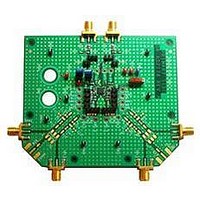
BOARD EVALUATION FOR AD8432
Manufacturer
Analog Devices Inc
Datasheet
1.AD8432-EVALZ.pdf
(28 pages)
Specifications of AD8432-EVALZ
Channels Per Ic
2 - Dual
Amplifier Type
Voltage Feedback
Output Type
Differential
Slew Rate
295 V/µs
-3db Bandwidth
200MHz
Current - Output / Channel
77mA
Operating Temperature
-40°C ~ 85°C
Current - Supply (main Ic)
24mA
Voltage - Supply, Single/dual (±)
4.5 V ~ 5.5 V
Board Type
Fully Populated
Utilized Ic / Part
AD8432
Silicon Manufacturer
Analog Devices
Application Sub Type
Noise Amplifier
Kit Application Type
Amplifier
Silicon Core Number
AD8432
Kit Contents
Board
Lead Free Status / RoHS Status
Lead free / RoHS Compliant


Table 5. Gain Setting Using a Pin-Strapping Technique and −3 dB Bandwidth for Each Gain Configuration
Differential
Gain (dB)
12.04
18.06
21.58
24.08
The single-ended gain from INH to OPH (see Figure 65) is
defined as
The single-ended gain from INH to OPL is defined as
The values of the seven gain resistors were chosen so that both
single-ended gains are equal. For example, to set a gain of
12.04 dB (G = ×4) differentially, the gain from INH to each
output (OPH, OPL) should be 6.02 dB (G = ×2).
INH to OPH: For R
INH to OPL: For R
ACTIVE INPUT RESISTANCE MATCHING
The AD8432 reduces noise and optimizes signal power transfer
by using active input termination to perform signal source
resistance matching.
The primary purpose of input impedance matching is to optimize
the input signal power transfer. With resistive termination, the
input noise increases due to the thermal noise of the terminating
resistor and the increased contribution of the input voltage
noise generator of the LNA. With active impedance matching,
however, the contributions of both are smaller than they are for
resistive termination by a factor of 1/(1 + ½ LNA) gain. The
noise figure (NF) for the three terminating schemes is shown in
Figure 67.
G
G
G
G
OPH
OPL
OPH
OPL
−
−
−
−
INH
INH
INH
INH
=
=
=
=
Single
Gain (dB)
6.02
12.04
15.56
18.06
−
−
R
R
R
R
G1
R
G1
G1
G1
G5
G5
R
G1
= R
+
+
= R
G1
+
R
R
=
R
G2
R
G
G2
G2
−
G6
R
G1
and R
+
2
= R
G1
=
−3 dB
BW (MHz)
200
90
50
32
+
×
R
R
2
G3
R
R
G
G
×
R
G7
G5
G
, then
+
G
R
= 2 × R
=
R
G
G4
−
=
2
2
G
RG1 (Ω)
12
12
12
12
, then
RG2 (Ω)
12
12
12
12
Rev. B | Page 19 of 28
RG3 (Ω)
Connect
GMH to GOH
24
Connect
GMH to GOH
24
To achieve this active impedance match, connect a feedback
resistor, R
given in Equation 1, where G/2 is the single-ended gain.
In addition, to further reduce the input resistance, there is an
internal resistance of 6.2 kΩ in parallel with the source resistance,
such that
Equation 3 should be used to calculate R
input resistance and single-ended gain. Refer to Table 6 for
calculated results for R
combinations.
⇒
R
R
IN
IN
R
RG4 (Ω)
Connect
GOH to OPH
Connect
GOH to OPH
48
48
=
=
FB
FB
V
V
V
, between the INH and OPL (see Figure 66). R
1
1+
IN
IN
IN
=
R
R
+
FB
FB
1
G
G
R
2
2
−
Figure 66. Input Resistance Matching
IN
R
R
R
R
R
S
S
S
+
INTERNAL
1
INTERNAL
R
R
R
R
IN
FB
IN
IN
IN
G
2
RG5 (Ω)
24
24
24
24
for several input resistance and gain
,
R
R
S
INH
INH
INH
INTERNAL
R
FB
IMPEDANCE MATCH
LNA
LNA
LNA
RG6 (Ω)
Connect
GML to GOL
24
Connect
GML to GOL
24
UNTERMINATED
TERMINATION
FB
RESISTIVE
=
ACTIVE
accurately for a desired
6
2 .
kΩ
V
V
V
OUT
OUT
OUT
AD8432
RG7 (Ω)
Connect
GOL to OPL
Connect
GOL to OPL
48
48
IN
is
(1)
(2)
(3)
Related parts for AD8432-EVALZ
Image
Part Number
Description
Manufacturer
Datasheet
Request
R


Part Number:
Description:
±1.7g Dual-Axis IMEMS Accelerometer Evaluation Board
Manufacturer:
Analog Devices Inc
Datasheet:

Part Number:
Description:
Inertial Sensor Evaluation System
Manufacturer:
Analog Devices Inc
Datasheet:
Part Number:
Description:
Manufacturer:
Analog Devices Inc
Datasheet:
Part Number:
Description:
Manufacturer:
Analog Devices Inc
Datasheet:
Part Number:
Description:
Manufacturer:
Analog Devices Inc
Datasheet:
Part Number:
Description:
Manufacturer:
Analog Devices Inc
Datasheet:
Part Number:
Description:
Manufacturer:
Analog Devices Inc
Datasheet:
Part Number:
Description:
Manufacturer:
Analog Devices Inc
Datasheet:
Part Number:
Description:
Manufacturer:
Analog Devices Inc
Datasheet:
Part Number:
Description:
Manufacturer:
Analog Devices Inc
Datasheet:
Part Number:
Description:
Manufacturer:
Analog Devices Inc
Datasheet:
Part Number:
Description:
Manufacturer:
Analog Devices Inc
Datasheet: