AD8432-EVALZ Analog Devices Inc, AD8432-EVALZ Datasheet - Page 21
AD8432-EVALZ
Manufacturer Part Number
AD8432-EVALZ
Description
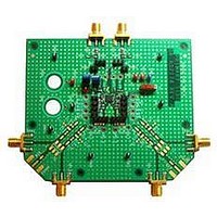
BOARD EVALUATION FOR AD8432
Manufacturer
Analog Devices Inc
Datasheet
1.AD8432-EVALZ.pdf
(28 pages)
Specifications of AD8432-EVALZ
Channels Per Ic
2 - Dual
Amplifier Type
Voltage Feedback
Output Type
Differential
Slew Rate
295 V/µs
-3db Bandwidth
200MHz
Current - Output / Channel
77mA
Operating Temperature
-40°C ~ 85°C
Current - Supply (main Ic)
24mA
Voltage - Supply, Single/dual (±)
4.5 V ~ 5.5 V
Board Type
Fully Populated
Utilized Ic / Part
AD8432
Silicon Manufacturer
Analog Devices
Application Sub Type
Noise Amplifier
Kit Application Type
Amplifier
Silicon Core Number
AD8432
Kit Contents
Board
Lead Free Status / RoHS Status
Lead free / RoHS Compliant


APPLICATIONS INFORMATION
The AD8432 LNA provides precision gain and ultralow noise
performance with minimal external components. Because it is
a high performance part, care must be taken to ensure that it is
configured optimally to attain the best performance and dynamic
range for the system.
TYPICAL SETUP
The internal bias circuitry of the AD8432 sets the input bias
voltage at 3.25 V and the output bias voltage at 2.5 V. It is important
to ac couple the inputs through a capacitor to maintain the internal
dc bias levels. When active input termination is used (R
decoupling capacitor (C
output bias voltages of the LNA. A typical value for C
a smaller value capacitor is more appropriate at higher frequencies.
IN1
IN2
FB
) is required to isolate the input and
120nH
120nH
FB
FB
R
R
FB1
FB2
R
15Ω
R
15Ω
C
47pF
C
47pF
SH1
SH2
0.1µF
0.1µF
SH1
SH2
0.1µF
0.1µF
0.1µF
0.1µF
C
C
FB1
FB2
Figure 69. Typical AD8432 Setup, G = 12.04 dB
FB
INH1
IND1
INL1
INH2
IND2
INL2
AD8432
is 0.1 μF, but
0.1µF
ENB
FB
120nH
FB
), a
Rev. B | Page 21 of 28
VPS1
BIAS
LNA1
LNA2
VPS2
The unterminated input impedance of the AD8432 is 6.2 kΩ.
Any input resistance between 50 Ω and 6.2 kΩ can be synthesized
using active impedance matching.
At the lowest gain (12.04 dB), the gain response exhibits some
peaking at higher frequencies. A resistor-capacitor shunt net-
work (RC) at the input (see RSHx and CSHx in Figure 69) is
recommended to reduce gain peaking and enhance stability at
higher frequencies.
Table 7 shows the recommended values of R
all four gains and several input impedance combinations. The
values for the C
and can be customized as needed to optimize performance. As
R
impedance values, no capacitor may be required.
0.1µF
IN
GMH1
GMH2
GOH1
GML1
GOH2
GML2
OPH1
GOL1
OPH2
GOL2
OPL1
OPL2
increases, the value of C
G = 12dB
COMM
SH
and R
R
R
L
L
SH
C
C
network are determined empirically
L
L
0.1µF
0.1µF
0.1µF
0.1µF
SH
diminishes, and for higher input
OUT1+
OUT1–
OUT2+
OUT2–
FB
, C
SH
, and R
AD8432
SH
for
Related parts for AD8432-EVALZ
Image
Part Number
Description
Manufacturer
Datasheet
Request
R


Part Number:
Description:
±1.7g Dual-Axis IMEMS Accelerometer Evaluation Board
Manufacturer:
Analog Devices Inc
Datasheet:

Part Number:
Description:
Inertial Sensor Evaluation System
Manufacturer:
Analog Devices Inc
Datasheet:
Part Number:
Description:
Manufacturer:
Analog Devices Inc
Datasheet:
Part Number:
Description:
Manufacturer:
Analog Devices Inc
Datasheet:
Part Number:
Description:
Manufacturer:
Analog Devices Inc
Datasheet:
Part Number:
Description:
Manufacturer:
Analog Devices Inc
Datasheet:
Part Number:
Description:
Manufacturer:
Analog Devices Inc
Datasheet:
Part Number:
Description:
Manufacturer:
Analog Devices Inc
Datasheet:
Part Number:
Description:
Manufacturer:
Analog Devices Inc
Datasheet:
Part Number:
Description:
Manufacturer:
Analog Devices Inc
Datasheet:
Part Number:
Description:
Manufacturer:
Analog Devices Inc
Datasheet:
Part Number:
Description:
Manufacturer:
Analog Devices Inc
Datasheet: