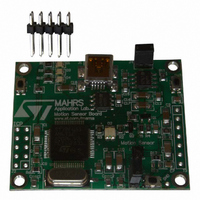
STEVAL-MKI024V1 STMicroelectronics, STEVAL-MKI024V1 Datasheet
STEVAL-MKI024V1
Specifications of STEVAL-MKI024V1
Available stocks


Related parts for STEVAL-MKI024V1


STEVAL-MKI024V1 Summary of contents
Page 1
Features ■ 2. 3.6 V supply voltage ■ 1.8 V compatible IOs ■ <1 mW power consumption ±2g / ±8g dynamically selectable full-scale ■ 2 ■ I C/SPI digital output ...
Page 2
Contents Contents 1 Block diagram and pin description . . . . . . . . . . . . . . . . . . . . . . . . . . . . . 6 1.1 Block ...
Page 3
LIS331DL 6 Register mapping . . . . . . . . . . . . . . . . . . . . . . . . . . . . . . . . . . . . ...
Page 4
Contents 9 Package information . . . . . . . . . . . . . . . . . . . . . . . . . . . . . . . . . . . . ...
Page 5
LIS331DL List of figures Figure 1. Block diagram . . . . . . . . . . . . . . . . . . . . . . . . . . . . . . . . ...
Page 6
List of tables List of tables Table 1. Device summary . . . . . . . . . . . . . . . . . . . . . . . . . . . . . . ...
Page 7
LIS331DL Table 49. CLICK_SRC register ...
Page 8
Block diagram and pin description 1 Block diagram and pin description 1.1 Block diagram Figure 1. Block diagram a SELF TEST 1.2 Pin description Figure 2. Pin connection X Y DIRECTION OF THE DETECTABLE ACCELERATIONS 8/ CHARGE AMPLIFIER ...
Page 9
LIS331DL Table 2. Pin description Pin Name Vdd_IO Power supply for I/O pins NC Internally Not Connected NC Internally Not Connected 2 SCL I ...
Page 10
Mechanical and electrical specifications 2 Mechanical and electrical specifications 2.1 Mechanical characteristics Table 3. Mechanical characteristics @ Vdd=2 °C unless otherwise noted Symbol Parameter FS Measurement range So Sensitivity Sensitivity change vs TCSo temperature Typical zero-g level ...
Page 11
LIS331DL 2.2 Electrical characteristics Table 4. Electrical characteristics @ Vdd=2 °C unless otherwise noted Symbol Parameter Vdd Supply voltage Vdd_IO I/O pins supply voltage Idd Supply current Current consumption in IddPdn power-down mode VIH Digital high level ...
Page 12
Mechanical and electrical specifications 2.3 Communication interface characteristics 2.3.1 SPI - serial peripheral interface Subject to general operating conditions for Vdd and top. Table 5. SPI slave timing values Symbol tc(SPC) SPI clock cycle fc(SPC) SPI clock frequency tsu(CS) CS ...
Page 13
LIS331DL 2 2.3 Inter IC control interface Subject to general operating conditions for Vdd and top. 2 Table slave timing values Symbol Parameter f SCL clock frequency (SCL) t SCL clock low time w(SCLL) ...
Page 14
Mechanical and electrical specifications 2.4 Absolute maximum ratings Stresses above those listed as “absolute maximum ratings” may cause permanent damage to the device. This is a stress rating only and functional operation of the device under these conditions is not ...
Page 15
LIS331DL 2.5 Terminology 2.5.1 Sensitivity Sensitivity describes the gain of the sensor and can be determined e.g. by applying 1 g acceleration to it. As the sensor can measure DC accelerations this can be done easily by pointing the axis ...
Page 16
Functionality 3 Functionality The LIS331DL is a nano, low-power, digital output 3-axis linear accelerometer packaged in an LGA package. The complete device includes a sensing element and an IC interface able to take the information from the sensing element and ...
Page 17
LIS331DL 4 Application hints Figure 5. LIS331DL electrical connection Vdd The device core is supplied through Vdd line while the I/O pads are supplied through Vdd_IO line. Power supply decoupling capacitors (100 nF ceramic, 10 µF Al) should be placed ...
Page 18
Digital interfaces 5 Digital interfaces The registers embedded inside the LIS331DL may be accessed through both the I SPI serial interfaces. The latter may be SW configured to operate either in 3-wire or 4-wire interface mode. The serial interfaces are ...
Page 19
LIS331DL 2 5.1 operation The transaction on the bus is started through a START (ST) signal. A START condition is defined as a HIGH to LOW transition on the data line while the SCL line is held HIGH. ...
Page 20
Digital interfaces Table 13. Transfer when Master is receiving (reading) one byte of data from slave Master ST SAD + W Slave Table 14. Transfer when Master is receiving (reading) multiple bytes of data from slave Master ST SAD+W SUB ...
Page 21
LIS331DL Both the Read Register and Write Register commands are completed in 16 clock pulses or in multiple case of multiple bytes read/write. Bit duration is the time between two falling edges of SPC. The first bit ...
Page 22
Digital interfaces Figure 8. Multiple bytes SPI read protocol (2 bytes example) CS SPC SDI RW MS SDO 5.2.2 SPI write Figure 9. SPI write protocol CS SPC SDI The SPI Write command is performed with 16 clock pulses. Multiple ...
Page 23
LIS331DL 5.2.3 SPI read in 3-wires mode 3-wires mode is entered by setting to 1 bit SIM (SPI Serial Interface Mode selection) in CTRL_REG2. Figure 11. SPI read protocol in 3-wires mode CS SPC SDI/O The SPI Read command is ...
Page 24
Register mapping 6 Register mapping The table given below provides a listing of the 8 bit registers embedded in the device and the related addresses: Table 15. Register address map Name Reserved (do not modify) WHO_AM_I Reserved (do not modify) ...
Page 25
LIS331DL Table 15. Register address map (continued) Name CLICK_THSZ CLICK_TimeLimit CLICK_Latency CLICK_Window Registers marked as “Reserved” must not be changed. The writing to those registers may cause permanent damages to the device. The content of the registers that are loaded ...
Page 26
Register description 7 Register description The device contains a set of registers which are used to control its behavior and to retrieve acceleration data. The registers address, made of 7 bits, is used to identify them and to write the ...
Page 27
LIS331DL Zen bit enables the generation of Data Ready signal for Z-axis measurement channel when set to 1. The default value is 1. Yen bit enables the generation of Data Ready signal for Y-axis measurement channel when set to 1. ...
Page 28
Register description Table 21. High pass filter cut-off frequency configuration HPcoeff2 7.4 CTRL_REG3 [interrupt CTRL register] (22h) Table 22. CTRL_REG3 register IHL PP_OD Table 23. CTRL_REG3 description IHL Interrupt active high, low. Default value 0. (0: ...
Page 29
LIS331DL 7.6 STATUS_REG (27h) Table 25. STATUS_REG register ZYXOR ZOR Table 26. STATUS_REG description axis Data Overrun. Default value: 0 ZYXOR (0: no overrun has occurred; 1: new data has overwritten the previous one before it was ...
Page 30
Register description 7.9 OUT_Z (2Dh) Table 29. OUT_Z register ZD7 ZD6 Z axis output data expressed as 2’s complement number. 7.10 FF_WU_CFG_1 (30h) Table 30. FF_WU_CFG_1 register AOI LIR Table 31. FF_WU_CFG_1 description And/Or combination of Interrupt events. Default value: ...
Page 31
LIS331DL 7.11 FF_WU_SRC_1 (31h) Table 32. FF_WU_SRC_1 register -- IA Table 33. FF_WU_SRC_1 description Interrupt Active. Default value (0: no interrupt has been generated; 1: one or more interrupts have been generated) Z High. Default value ...
Page 32
Register description 7.13 FF_WU_DURATION_1 (33h) Table 36. FF_WU_DURATION_1 register D7 D6 Table 37. FF_WU_DURATION_1 description D7-D0 Duration register for Free-Fall/Wake-Up interrupt 1. Duration step and maximum value depend on the ODR chosen. Step 2.5 msec, from 0 to 637.5 msec ...
Page 33
LIS331DL 7.15 FF_WU_SRC_2 (35h) Table 40. FF_WU_SRC_2 register -- IA Table 41. FF_WU_SRC_2 description IA Interrupt Active. Default value: 0 (0: no interrupt has been generated; 1: one or more interrupt events have been generated High. Default value: ...
Page 34
Register description 7.17 FF_WU_DURATION_2 (37h) Table 44. FF_WU_DURATION_2 register D7 D6 Table 45. FF_WU_DURATION_2 description D7-D0 Duration value. Default value: 0000 0000 Duration register for Free-Fall/Wake-Up interrupt 2. Duration step and maximum value depend on the ODR chosen. Step 2.5 ...
Page 35
LIS331DL Table 48. Click interrupt configurations Double_Z / 7.19 CLICK_SRC (39h) Table 49. CLICK_SRC register -- IA Table 50. CLICK_SRC description IA Interrupt Active. Default value: 0 (0: no interrupt has been generated; ...
Page 36
Register description 7.21 CLICK_THSZ (3Ch) Table 53. CLICK_THSZ register -- -- Table 54. CLICK_THSZ description THSz3, THSz0 Click Threshold on Z axis. Default value: 0000 From 0.5 g (0001) to 7.5 g (1111) with step of 0.5 g. 7.22 CLICK_TimeLimit ...
Page 37
LIS331DL 8 Typical performance characteristics 8.1 Mechanical characteristics at 25 °C Figure 12. X axis Zero-g level at 2 −150 −100 −50 0 Zero−g Level Offset [mg] Figure 14. Y axis Zero-g level ...
Page 38
Typical performance characteristics 8.2 Mechanical characteristics derived from measurement in the -40 °C to +85 °C temperature range Figure 18. X axis Zero-g level change vs. temperature at 2 −4 −3 −2 ...
Page 39
LIS331DL 8.3 Electrical characteristics at 25 °C Figure 24. Current consumption in normal mode at 2 200 220 240 260 280 300 Current consumption [uA] 320 340 360 ...
Page 40
Package information 9 Package information In order to meet environmental requirements, ST offers these devices in ECOPACK packages. These packages have a lead-free second level interconnect. The category of second Level Interconnect is marked on the inner box label, in ...
Page 41
LIS331DL 10 Revision history Table 58. Document revision history Date 28-Sep-2007 21-Jan-2008 16-Apr-2008 Revision 1 Initial release Updated package specification and package dimensions on page 2 Minor text changes to improve readability. Updated paragraph 2.1: Mechanical characteristics 3 section 8: ...
Page 42
... Information in this document is provided solely in connection with ST products. STMicroelectronics NV and its subsidiaries (“ST”) reserve the right to make changes, corrections, modifications or improvements, to this document, and the products and services described herein at any time, without notice. All ST products are sold pursuant to ST’s terms and conditions of sale. ...