ADIS16265/PCBZ Analog Devices Inc, ADIS16265/PCBZ Datasheet - Page 15
ADIS16265/PCBZ
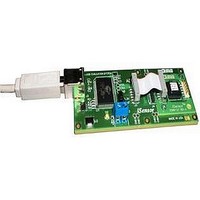
Manufacturer Part Number
ADIS16265/PCBZ
Description
BOARD EVALUATION FOR ADIS16265
Manufacturer
Analog Devices Inc
Series
iMEMS®, iSensor™r
Datasheet
1.ADIS16260PCBZ.pdf
(20 pages)
Specifications of ADIS16265/PCBZ
Sensor Type
Gyroscope, 1 Axis
Sensing Range
±80°/sec, ±160°/sec, ±320°/sec
Sensitivity
±0.2%
Embedded
No
Utilized Ic / Part
ADIS16265
Silicon Manufacturer
Analog Devices
Application Sub Type
Angular Rate Sensor / Gyroscope
Kit Application Type
Sensing - Motion / Vibration / Shock
Silicon Core Number
ADIS16265
Lead Free Status / RoHS Status
Lead free / RoHS compliant by exemption
Voltage - Supply
-
Interface
-
Lead Free Status / RoHS Status
Lead free / RoHS compliant by exemption


Global Commands
The GLOB_CMD register provides trigger bits for several
functions. Setting the assigned bit to 1 starts each operation,
which returns the bit to 0 after completion. For example, set
GLOB_CMD[7] = 1 (DIN = 0xBE80) to execute a software
reset, which stops the sensor operation and runs the device
through its start-up sequence. This sequence includes loading
the control registers with the contents of their respective flash
memory locations prior to producing new data.
Table 18. GLOB_CMD Bit Descriptions
Bits
[15:8]
[7]
[6:4]
[3]
[2]
[1]
[0]
Power Management
Setting SMPL_PRD[7:0] ≥ 0x08 also sets the sensor to low
power mode. For systems that require lower power dissipation,
in-system characterization helps users to quantify the associated
performance trade-offs. In addition to sensor performance, low
power mode affects SPI data rates (see Table 2). Use SLP_CNT[7:0]
to put the device into sleep mode for a specified period. For
example, SLP_CNT[7:0] = 0x64 (DIN = 0xBA64) puts the
ADIS16260 and ADIS16265 to sleep for 50 seconds.
Table 19. SLP_CNT Bit Descriptions
Bits
[15:8]
[7:0]
INPUT/OUTPUT FUNCTIONS
General-Purpose I/O
DIO1 and DIO2 are configurable, general-purpose I/O lines
that serve multiple purposes according to the following control
register priority: MSC_CTRL, ALM_CTRL, and GPIO_CTRL.
For example, set GPIO_CTRL = 0x0202 (DIN = 0xB302, and
then 0xB202) to configure DIO1 as an input and DIO2 as an
output set high.
Table 20. GPIO_CTRL Bit Descriptions
Bits
[15:10]
[9]
[8]
[7:2]
[1]
[0]
Description
Not used.
Software reset command.
Not used.
Flash update command.
Auxiliary DAC data latch.
Factory calibration restore command.
Autonull command.
Description (Default = 0x0000)
Not used.
Programmable sleep time bits, 0.5 sec/LSB.
Description
Not used.
General-Purpose I/O Line 2 (DIO2) data level.
General-Purpose I/O Line 1 (DIO1) data level.
Not used.
General-Purpose I/O Line 2 (DIO2) direction control.
1 = output, 0 = input.
General-Purpose I/O Line 1 (DIO1) direction control.
1 = output, 0 = input.
Rev. B | Page 15 of 20
Data Ready I/O Indicator
The MSC_CTRL[2:0] bits configure one of the digital I/O lines
as a data ready signal for driving an interrupt. For example, set
MSC_CTRL[2:0] = 100 (DIN = 0xB404) to configure DIO1 as
a negative-pulse data ready signal. The pulse width is between
100 µs and 200 µs over all conditions.
Table 21. MSC_CTRL Bit Descriptions
Bits
[15:12]
[11]
[10]
[9]
[8]
[7:3]
[2]
[1]
[0]
Auxiliary DAC
The 12-bit AUX_DAC line can drive its output to within 5 mV
of the ground reference when it is not sinking current. As the
output approaches 0 V, the linearity begins to degrade (~100 LSB
starting point). As the sink current increases, the nonlinear
range increases. The DAC latch command moves the values of
the AUX_DAC register into the DAC input register, enabling
both bytes to take effect at the same time.
Table 22. AUX_DAC Bit Descriptions
Bits
[15:12]
[11:0]
Table 23. Setting AUX_DAC = 2 V
DIN
0xB0CC
0xB10C
0xBE04
Description (Default = 0x0000)
Not used.
Memory test (cleared upon completion).
1 = enabled, 0 = disabled.
Internal self-test enable (cleared upon completion).
1 = enabled, 0 = disabled.
Manual self-test, negative stimulus.
1 = enabled, 0 = disabled.
Manual self-test, positive stimulus.
1 = enabled, 0 = disabled.
Not used.
Data ready enable.
1 = enabled, 0 = disabled.
Data ready polarity.
1 = active high, 0 = active low.
Data ready line select.
1 = DIO2, 0 = DIO1.
Description (Default = 0x0000)
Not used.
Data bits, scale factor = 0.6105 mV/code.
Offset binary format, 0 V = 0 codes.
Description
AUX_DAC[7:0] = 0xCC (204 LSB).
AUX_DAC[15:8] = 0x0C (3072 LSB).
GLOB_CMD[2] = 1.
Move values into the DAC input register, resulting in
a 2 V output level.
ADIS16260/ADIS16265
Related parts for ADIS16265/PCBZ
Image
Part Number
Description
Manufacturer
Datasheet
Request
R

Part Number:
Description:
±1.7g Dual-Axis IMEMS Accelerometer Evaluation Board
Manufacturer:
Analog Devices Inc
Datasheet:

Part Number:
Description:
Inertial Sensor Evaluation System
Manufacturer:
Analog Devices Inc
Datasheet:
Part Number:
Description:
Manufacturer:
Analog Devices Inc
Datasheet:
Part Number:
Description:
Manufacturer:
Analog Devices Inc
Datasheet:
Part Number:
Description:
Manufacturer:
Analog Devices Inc
Datasheet:
Part Number:
Description:
Manufacturer:
Analog Devices Inc
Datasheet:
Part Number:
Description:
Manufacturer:
Analog Devices Inc
Datasheet:
Part Number:
Description:
Manufacturer:
Analog Devices Inc
Datasheet:
Part Number:
Description:
Manufacturer:
Analog Devices Inc
Datasheet:
Part Number:
Description:
Manufacturer:
Analog Devices Inc
Datasheet:
Part Number:
Description:
Manufacturer:
Analog Devices Inc
Datasheet:
Part Number:
Description:
Manufacturer:
Analog Devices Inc
Datasheet:
Part Number:
Description:
Manufacturer:
Analog Devices Inc
Datasheet: