ADIS16265/PCBZ Analog Devices Inc, ADIS16265/PCBZ Datasheet - Page 4
ADIS16265/PCBZ
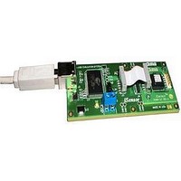
Manufacturer Part Number
ADIS16265/PCBZ
Description
BOARD EVALUATION FOR ADIS16265
Manufacturer
Analog Devices Inc
Series
iMEMS®, iSensor™r
Datasheet
1.ADIS16260PCBZ.pdf
(20 pages)
Specifications of ADIS16265/PCBZ
Sensor Type
Gyroscope, 1 Axis
Sensing Range
±80°/sec, ±160°/sec, ±320°/sec
Sensitivity
±0.2%
Embedded
No
Utilized Ic / Part
ADIS16265
Silicon Manufacturer
Analog Devices
Application Sub Type
Angular Rate Sensor / Gyroscope
Kit Application Type
Sensing - Motion / Vibration / Shock
Silicon Core Number
ADIS16265
Lead Free Status / RoHS Status
Lead free / RoHS compliant by exemption
Voltage - Supply
-
Interface
-
Lead Free Status / RoHS Status
Lead free / RoHS compliant by exemption


ADIS16260/ADIS16265
Parameter
DAC OUTPUT
LOGIC INPUTS
DIGITAL OUTPUTS
SLEEP TIMER
START-UP TIME
FLASH MEMORY
CONVERSION RATE
POWER SUPPLY
1
2
3
4
5
ADIS16260/ADIS16265 characterization data represents ±4σ to fall within the ±1% limit.
The maximum guaranteed measurement range is ±320°/sec. The sensor outputs will measure beyond this range, but performance is not assured.
Guaranteed by design.
Endurance is qualified as per JEDEC Standard 22, Method A117, and measured at −40°C, +25°C, +85°C, and +125°C.
Retention lifetime equivalent at a junction temperature (T
Resolution
Relative Accuracy
Differential Nonlinearity
Offset Error
Gain Error
Output Range
Output Impedance
Output Settling Time
Input High Voltage, V
Input Low Voltage, V
Logic 1 Input Current, I
Logic 0 Input Current, I
Input Capacitance, C
Output High Voltage, V
Output Low Voltage, V
Timeout Period
Initial Start-Up Time
Sleep Mode Recovery
Flash Update Time
Flash Test Process Time
Endurance
Data Retention
Minimum Conversion Time
Maximum Conversion Time
Maximum Throughput Rate
Minimum Throughput Rate
Operating Voltage Range, V
Power Supply Current
All Except RST
RST
4
5
3
INL
IN
INH
OL
INH
INL
OH
CC
Test Conditions/Comments
5 kΩ/100 pF to GND
For Code 101 to Code 4095
Internal 3.3 V interface
V
V
The RST pin has an internal pull-up.
Internal 3.3 V interface
I
I
Normal mode, SMPL_PRD[7:0] ≤ 0x07
Low power mode, SMPL_PRD[7:0] ≥ 0x08
T
SMPL_PRD[7:0] = 0x00
SMPL_PRD[7:0] = 0xFF
SMPL_PRD[7:0] = 0x00
SMPL_PRD[7:0] = 0xFF
Low power mode, SMPL_PRD[7:0] ≥ 0x08
Normal mode, SMPL_PRD[7:0] ≤ 0x07
Sleep mode
SOURCE
SINK
J
IH
IL
= 55°C
= 0 V
= 3.3 V
= 1.6 mA
= 1.6 mA
J
) of 55°C, as per JEDEC Standard 22, Method A117. Retention lifetime decreases with junction temperature.
Rev. B | Page 4 of 20
Min
0
2.0
2.4
0.5
20,000
10
4.75
12
4
1
±5
±0.5
2
10
±0.2
−40
−1
10
165
2.5
50
18
70
0.488
7.75
2048
0.129
5.0
17
41
350
Typ
2.5
0.8
±10
−60
0.4
128
5.25
Max
%
µA
V
V
sec
ms
ms
Cycles
Years
ms
SPS
SPS
µA
Unit
Bits
LSB
LSB
mV
V
Ω
µs
V
V
µA
mA
pF
ms
ms
ms
sec
V
mA
mA
Related parts for ADIS16265/PCBZ
Image
Part Number
Description
Manufacturer
Datasheet
Request
R

Part Number:
Description:
±1.7g Dual-Axis IMEMS Accelerometer Evaluation Board
Manufacturer:
Analog Devices Inc
Datasheet:

Part Number:
Description:
Inertial Sensor Evaluation System
Manufacturer:
Analog Devices Inc
Datasheet:
Part Number:
Description:
Manufacturer:
Analog Devices Inc
Datasheet:
Part Number:
Description:
Manufacturer:
Analog Devices Inc
Datasheet:
Part Number:
Description:
Manufacturer:
Analog Devices Inc
Datasheet:
Part Number:
Description:
Manufacturer:
Analog Devices Inc
Datasheet:
Part Number:
Description:
Manufacturer:
Analog Devices Inc
Datasheet:
Part Number:
Description:
Manufacturer:
Analog Devices Inc
Datasheet:
Part Number:
Description:
Manufacturer:
Analog Devices Inc
Datasheet:
Part Number:
Description:
Manufacturer:
Analog Devices Inc
Datasheet:
Part Number:
Description:
Manufacturer:
Analog Devices Inc
Datasheet:
Part Number:
Description:
Manufacturer:
Analog Devices Inc
Datasheet:
Part Number:
Description:
Manufacturer:
Analog Devices Inc
Datasheet: