C8051F120DK Silicon Laboratories Inc, C8051F120DK Datasheet - Page 105
C8051F120DK
Manufacturer Part Number
C8051F120DK
Description
DEVKIT-F120/21/22/23/24/25/26/27
Manufacturer
Silicon Laboratories Inc
Type
MCUr
Datasheet
1.C8051F120DK.pdf
(350 pages)
Specifications of C8051F120DK
Contents
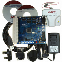
Evaluation Board, Power Supply, USB Cables, Adapter and Documentation
Processor To Be Evaluated
C8051F12x and C8051F13x
Interface Type
USB
Silicon Manufacturer
Silicon Labs
Core Architecture
8051
Silicon Core Number
C8051F120
Silicon Family Name
C8051F12x
Lead Free Status / RoHS Status
Contains lead / RoHS non-compliant
For Use With/related Products
C8051F120, 121, 122, 123, 124, 125, 126, 127
Lead Free Status / Rohs Status
Lead free / RoHS Compliant
Other names
336-1224
Available stocks
Company
Part Number
Manufacturer
Quantity
Price
Company:

Part Number:
C8051F120DK
Manufacturer:
SiliconL
Quantity:
4


8.
The C8051F12x devices include two on-chip 12-bit voltage-mode Digital-to-Analog Converters (DACs).
Each DAC has an output swing of 0 V to (VREF-1LSB) for a corresponding input code range of 0x000 to
0xFFF. The DACs may be enabled/disabled via their corresponding control registers, DAC0CN and
DAC1CN. While disabled, the DAC output is maintained in a high-impedance state, and the DAC supply
current falls to 1 µA or less. The voltage reference for each DAC is supplied at the VREFD pin
(C8051F120/2/4/6 devices) or the VREF pin (C8051F121/3/5/7 devices). Note that the VREF pin on
C8051F121/3/5/7 devices may be driven by the internal voltage reference or an external source. If the
internal voltage reference is used it must be enabled in order for the DAC outputs to be valid. See
“9. Voltage Reference” on page 113
DACs.
8.1.
Each DAC features a flexible output update mechanism which allows for seamless full-scale changes and
supports jitter-free updates for waveform generation. The following examples are written in terms of DAC0,
but DAC1 operation is identical.
DACs, 12-Bit Voltage Mode (C8051F12x Only)
DAC Output Scheduling
DAC0MD1
DAC0MD0
DAC1MD1
DAC1MD0
DAC0DF2
DAC0DF1
DAC0DF0
DAC1DF2
DAC1DF1
DAC1DF0
DAC0EN
DAC1EN
Figure 8.1. DAC Functional Block Diagram
8
8
8
8
8
8
8
8
for more information on configuring the voltage reference for the
12
12
Rev. 1.4
REF
REF
DAC0
DAC1
C8051F120/1/2/3/4/5/6/7
C8051F130/1/2/3
AGND
AGND
AV+
AV+
DAC0
DAC1
Section
105
Related parts for C8051F120DK
Image
Part Number
Description
Manufacturer
Datasheet
Request
R

Part Number:
Description:
SMD/C°/SINGLE-ENDED OUTPUT SILICON OSCILLATOR
Manufacturer:
Silicon Laboratories Inc
Part Number:
Description:
Manufacturer:
Silicon Laboratories Inc
Datasheet:
Part Number:
Description:
N/A N/A/SI4010 AES KEYFOB DEMO WITH LCD RX
Manufacturer:
Silicon Laboratories Inc
Datasheet:
Part Number:
Description:
N/A N/A/SI4010 SIMPLIFIED KEY FOB DEMO WITH LED RX
Manufacturer:
Silicon Laboratories Inc
Datasheet:
Part Number:
Description:
N/A/-40 TO 85 OC/EZLINK MODULE; F930/4432 HIGH BAND (REV E/B1)
Manufacturer:
Silicon Laboratories Inc
Part Number:
Description:
EZLink Module; F930/4432 Low Band (rev e/B1)
Manufacturer:
Silicon Laboratories Inc
Part Number:
Description:
I°/4460 10 DBM RADIO TEST CARD 434 MHZ
Manufacturer:
Silicon Laboratories Inc
Part Number:
Description:
I°/4461 14 DBM RADIO TEST CARD 868 MHZ
Manufacturer:
Silicon Laboratories Inc
Part Number:
Description:
I°/4463 20 DBM RFSWITCH RADIO TEST CARD 460 MHZ
Manufacturer:
Silicon Laboratories Inc
Part Number:
Description:
I°/4463 20 DBM RADIO TEST CARD 868 MHZ
Manufacturer:
Silicon Laboratories Inc
Part Number:
Description:
I°/4463 27 DBM RADIO TEST CARD 868 MHZ
Manufacturer:
Silicon Laboratories Inc
Part Number:
Description:
I°/4463 SKYWORKS 30 DBM RADIO TEST CARD 915 MHZ
Manufacturer:
Silicon Laboratories Inc
Part Number:
Description:
N/A N/A/-40 TO 85 OC/4463 RFMD 30 DBM RADIO TEST CARD 915 MHZ
Manufacturer:
Silicon Laboratories Inc
Part Number:
Description:
I°/4463 20 DBM RADIO TEST CARD 169 MHZ
Manufacturer:
Silicon Laboratories Inc