C8051F120DK Silicon Laboratories Inc, C8051F120DK Datasheet - Page 133
C8051F120DK
Manufacturer Part Number
C8051F120DK
Description
DEVKIT-F120/21/22/23/24/25/26/27
Manufacturer
Silicon Laboratories Inc
Type
MCUr
Datasheet
1.C8051F120DK.pdf
(350 pages)
Specifications of C8051F120DK
Contents
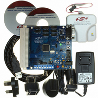
Evaluation Board, Power Supply, USB Cables, Adapter and Documentation
Processor To Be Evaluated
C8051F12x and C8051F13x
Interface Type
USB
Silicon Manufacturer
Silicon Labs
Core Architecture
8051
Silicon Core Number
C8051F120
Silicon Family Name
C8051F12x
Lead Free Status / RoHS Status
Contains lead / RoHS non-compliant
For Use With/related Products
C8051F120, 121, 122, 123, 124, 125, 126, 127
Lead Free Status / Rohs Status
Lead free / RoHS Compliant
Other names
336-1224
Available stocks
Company
Part Number
Manufacturer
Quantity
Price
Company:

Part Number:
C8051F120DK
Manufacturer:
SiliconL
Quantity:
4


11.2. Memory Organization
The memory organization of the CIP-51 System Controller is similar to that of a standard 8051. There are
two separate memory spaces: program memory and data memory. Program and data memory share the
same address space but are accessed via different instruction types. There are 256 bytes of internal data
memory and 128k bytes (C8051F12x and C8051F130/1) or 64k bytes (C8051F132/3) of internal program
memory address space implemented within the CIP-51. The CIP-51 memory organization is shown in
Figure 11.2.
11.2.1. Program Memory
The C8051F12x and C8051F130/1 have a 128 kB program memory space. The MCU implements this pro-
gram memory space as in-system re-programmable Flash memory in four 32 kB code banks. A common
code bank (Bank 0) of 32 kB is always accessible from addresses 0x0000 to 0x7FFF. The three upper
code banks (Bank 1, Bank 2, and Bank 3) are each mapped to addresses 0x8000 to 0xFFFF, depending
on the selection of bits in the PSBANK register, as described in SFR Definition 11.1. The IFBANK bits
select which of the upper banks are used for code execution, while the COBANK bits select the bank to be
used for direct writes and reads of the Flash memory. Note: 1024 bytes of the memory in Bank 3
(0x1FC00 to 0x1FFFF) are reserved and are not available for user program or data storage. The
C8051F132/3 have a 64k byte program memory space implemented as in-system re-programmable Flash
memory, and organized in a contiguous block from address 0x00000 to 0x0FFFF.
Program memory is normally assumed to be read-only. However, the CIP-51 can write to program memory
by setting the Program Store Write Enable bit (PSCTL.0) and using the MOVX instruction. This feature pro-
vides a mechanism for the CIP-51 to update program code and use the program memory space for non-
volatile data storage. Refer to
0x1FFFF
0x1FC00
0x1FBFF
0x0FFFF
0x200FF
0x200FF
0x20000
0x20000
0x00000
0x00000
PROGRAM/DATA MEMORY
C8051F120/1/2/3/4/5/6/7
Programmable in 1024
Programmable in 1024
(FLASH)
Scrachpad Memory
Scrachpad Memory
C8051F130/1
C8051F132/3
Byte Sectors)
Byte Sectors)
(DATA only)
RESERVED
(DATA only)
(In-System
(In-System
FLASH
FLASH
Section “15. Flash Memory” on page 199
Figure 11.2. Memory Map
(Indirect Addressing
(Direct and Indirect
Rev. 1.4
General Purpose
Upper 128 RAM
Bit Addressable
Addressing)
Registers
EXTERNAL DATA ADDRESS SPACE
0xFFFF
0x1FFF
0x2000
0x0000
INTERNAL DATA ADDRESS SPACE
Only)
DATA MEMORY (RAM)
C8051F120/1/2/3/4/5/6/7
XRAM - 8192 Bytes
(accessable using MOVX
Off-chip XRAM space
instruction)
(Direct Addressing Only)
Lower 128 RAM
(Direct and Indirect
Addressing)
Special Function
Registers
C8051F130/1/2/3
for further details.
0
256 SFR Pages
1
2
3
Up To
133
Related parts for C8051F120DK
Image
Part Number
Description
Manufacturer
Datasheet
Request
R

Part Number:
Description:
SMD/C°/SINGLE-ENDED OUTPUT SILICON OSCILLATOR
Manufacturer:
Silicon Laboratories Inc
Part Number:
Description:
Manufacturer:
Silicon Laboratories Inc
Datasheet:
Part Number:
Description:
N/A N/A/SI4010 AES KEYFOB DEMO WITH LCD RX
Manufacturer:
Silicon Laboratories Inc
Datasheet:
Part Number:
Description:
N/A N/A/SI4010 SIMPLIFIED KEY FOB DEMO WITH LED RX
Manufacturer:
Silicon Laboratories Inc
Datasheet:
Part Number:
Description:
N/A/-40 TO 85 OC/EZLINK MODULE; F930/4432 HIGH BAND (REV E/B1)
Manufacturer:
Silicon Laboratories Inc
Part Number:
Description:
EZLink Module; F930/4432 Low Band (rev e/B1)
Manufacturer:
Silicon Laboratories Inc
Part Number:
Description:
I°/4460 10 DBM RADIO TEST CARD 434 MHZ
Manufacturer:
Silicon Laboratories Inc
Part Number:
Description:
I°/4461 14 DBM RADIO TEST CARD 868 MHZ
Manufacturer:
Silicon Laboratories Inc
Part Number:
Description:
I°/4463 20 DBM RFSWITCH RADIO TEST CARD 460 MHZ
Manufacturer:
Silicon Laboratories Inc
Part Number:
Description:
I°/4463 20 DBM RADIO TEST CARD 868 MHZ
Manufacturer:
Silicon Laboratories Inc
Part Number:
Description:
I°/4463 27 DBM RADIO TEST CARD 868 MHZ
Manufacturer:
Silicon Laboratories Inc
Part Number:
Description:
I°/4463 SKYWORKS 30 DBM RADIO TEST CARD 915 MHZ
Manufacturer:
Silicon Laboratories Inc
Part Number:
Description:
N/A N/A/-40 TO 85 OC/4463 RFMD 30 DBM RADIO TEST CARD 915 MHZ
Manufacturer:
Silicon Laboratories Inc
Part Number:
Description:
I°/4463 20 DBM RADIO TEST CARD 169 MHZ
Manufacturer:
Silicon Laboratories Inc