C8051F120DK Silicon Laboratories Inc, C8051F120DK Datasheet - Page 200
C8051F120DK
Manufacturer Part Number
C8051F120DK
Description
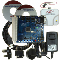
DEVKIT-F120/21/22/23/24/25/26/27
Manufacturer
Silicon Laboratories Inc
Type
MCUr
Datasheet
1.C8051F120DK.pdf
(350 pages)
Specifications of C8051F120DK
Contents
Evaluation Board, Power Supply, USB Cables, Adapter and Documentation
Processor To Be Evaluated
C8051F12x and C8051F13x
Interface Type
USB
Silicon Manufacturer
Silicon Labs
Core Architecture
8051
Silicon Core Number
C8051F120
Silicon Family Name
C8051F12x
Lead Free Status / RoHS Status
Contains lead / RoHS non-compliant
For Use With/related Products
C8051F120, 121, 122, 123, 124, 125, 126, 127
Lead Free Status / Rohs Status
Lead free / RoHS Compliant
Other names
336-1224
Available stocks
Company
Part Number
Manufacturer
Quantity
Price
Company:

Part Number:
C8051F120DK
Manufacturer:
SiliconL
Quantity:
4


C8051F120/1/2/3/4/5/6/7
C8051F130/1/2/3
15.1.1. Non-volatile Data Storage
The Flash memory can be used for non-volatile data storage as well as program code. This allows data
such as calibration coefficients to be calculated and stored at run time. Data is written and erased using the
MOVX write instruction (as described in
instruction. The COBANK bits in register PSBANK (SFR Definition 11.1) control which portion of the Flash
memory is targeted by writes and erases of addresses above 0x07FFF. For devices with 64 kB of Flash.
the COBANK bits should always remain set to ‘01’ to ensure that Flash write, erase, and read operations
are valid.
Two additional 128-byte sectors (256 bytes total) of Flash memory are included for non-volatile data stor-
age. The smaller sector size makes them particularly well suited as general purpose, non-volatile scratch-
pad memory. Even though Flash memory can be written a single byte at a time, an entire sector must be
erased first. In order to change a single byte of a multi-byte data set, the data must be moved to temporary
storage. The 128-byte sector-size facilitates updating data without wasting program memory or RAM
space. The 128-byte sectors are double-mapped over the normal Flash memory for MOVC reads and
MOVX writes only; their addresses range from 0x00 to 0x7F and from 0x80 to 0xFF (see Figure 15.2). To
access the 128-byte sectors, the SFLE bit in PSCTL must be set to logic 1. Code execution from the 128-
byte Scratchpad areas is not permitted. The 128-byte sectors can be erased individually, or both at the
same time. To erase both sectors simultaneously, the address 0x0400 should be targeted during the erase
operation with SFLE set to ‘1’. See Figure 15.1 for the memory map under different COBANK and SFLE
settings.
200
V
Flash Size
Flash Size
Endurance
Erase Cycle Time
Write Cycle Time
Notes:
DD
1. Includes 256-byte Scratch Pad Area
2. 1024 Bytes at location 0x1FC00 to 0x1FFFF are reserved.
= 2.7 to 3.6 V; –40 to +85 °C
Parameter
1
1
C8051F12x and C8051F130/1
C8051F132/3
Table 15.1. Flash Electrical Characteristics
Conditions
Section 15.1.2
Rev. 1.4
and
Section 15.1.3
Min
20k
10
40
131328
65792
100k
Typ
12
50
) and read using the MOVC
2
Max
14
60
Erase/Write
Units
Bytes
Bytes
ms
µs
Related parts for C8051F120DK
Image
Part Number
Description
Manufacturer
Datasheet
Request
R

Part Number:
Description:
SMD/C°/SINGLE-ENDED OUTPUT SILICON OSCILLATOR
Manufacturer:
Silicon Laboratories Inc
Part Number:
Description:
Manufacturer:
Silicon Laboratories Inc
Datasheet:
Part Number:
Description:
N/A N/A/SI4010 AES KEYFOB DEMO WITH LCD RX
Manufacturer:
Silicon Laboratories Inc
Datasheet:
Part Number:
Description:
N/A N/A/SI4010 SIMPLIFIED KEY FOB DEMO WITH LED RX
Manufacturer:
Silicon Laboratories Inc
Datasheet:
Part Number:
Description:
N/A/-40 TO 85 OC/EZLINK MODULE; F930/4432 HIGH BAND (REV E/B1)
Manufacturer:
Silicon Laboratories Inc
Part Number:
Description:
EZLink Module; F930/4432 Low Band (rev e/B1)
Manufacturer:
Silicon Laboratories Inc
Part Number:
Description:
I°/4460 10 DBM RADIO TEST CARD 434 MHZ
Manufacturer:
Silicon Laboratories Inc
Part Number:
Description:
I°/4461 14 DBM RADIO TEST CARD 868 MHZ
Manufacturer:
Silicon Laboratories Inc
Part Number:
Description:
I°/4463 20 DBM RFSWITCH RADIO TEST CARD 460 MHZ
Manufacturer:
Silicon Laboratories Inc
Part Number:
Description:
I°/4463 20 DBM RADIO TEST CARD 868 MHZ
Manufacturer:
Silicon Laboratories Inc
Part Number:
Description:
I°/4463 27 DBM RADIO TEST CARD 868 MHZ
Manufacturer:
Silicon Laboratories Inc
Part Number:
Description:
I°/4463 SKYWORKS 30 DBM RADIO TEST CARD 915 MHZ
Manufacturer:
Silicon Laboratories Inc
Part Number:
Description:
N/A N/A/-40 TO 85 OC/4463 RFMD 30 DBM RADIO TEST CARD 915 MHZ
Manufacturer:
Silicon Laboratories Inc
Part Number:
Description:
I°/4463 20 DBM RADIO TEST CARD 169 MHZ
Manufacturer:
Silicon Laboratories Inc