C8051F120DK Silicon Laboratories Inc, C8051F120DK Datasheet - Page 202
C8051F120DK
Manufacturer Part Number
C8051F120DK
Description
DEVKIT-F120/21/22/23/24/25/26/27
Manufacturer
Silicon Laboratories Inc
Type
MCUr
Datasheet
1.C8051F120DK.pdf
(350 pages)
Specifications of C8051F120DK
Contents
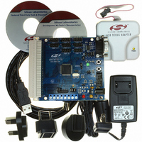
Evaluation Board, Power Supply, USB Cables, Adapter and Documentation
Processor To Be Evaluated
C8051F12x and C8051F13x
Interface Type
USB
Silicon Manufacturer
Silicon Labs
Core Architecture
8051
Silicon Core Number
C8051F120
Silicon Family Name
C8051F12x
Lead Free Status / RoHS Status
Contains lead / RoHS non-compliant
For Use With/related Products
C8051F120, 121, 122, 123, 124, 125, 126, 127
Lead Free Status / Rohs Status
Lead free / RoHS Compliant
Other names
336-1224
Available stocks
Company
Part Number
Manufacturer
Quantity
Price
Company:

Part Number:
C8051F120DK
Manufacturer:
SiliconL
Quantity:
4


C8051F120/1/2/3/4/5/6/7
C8051F130/1/2/3
15.1.3. Writing Flash Memory From Software
Bytes in Flash memory can be written one byte at a time, or in small blocks. The CHBLKW bit in register
CCH0CN (SFR Definition 16.1) controls whether a single byte or a block of bytes is written to Flash during
a write operation. When CHBLKW is cleared to ‘0’, the Flash will be written one byte at a time. When
CHBLKW is set to ‘1’, the Flash will be written in blocks of four bytes for addresses in code space, or
blocks of two bytes for addresses in the Scratchpad area. Block writes are performed in the same amount
of time as single byte writes, which can save time when storing large amounts of data to Flash memory.
For single-byte writes to Flash, bytes are written individually, and the Flash write is performed after each
MOVX write instruction. The recommended procedure for writing Flash in single bytes is as follows:
For block Flash writes, the Flash write procedure is only performed after the last byte of each block is writ-
ten with the MOVX write instruction. When writing to addresses located in any of the four code banks, a
Flash write block is four bytes long, from addresses ending in 00b to addresses ending in 11b. Writes must
be performed sequentially (i.e. addresses ending in 00b, 01b, 10b, and 11b must be written in order). The
Flash write will be performed following the MOVX write that targets the address ending in 11b. When writ-
ing to addresses located in the Flash Scratchpad area, a Flash block is two bytes long, from addresses
ending in 0b to addresses ending in 1b. The Flash write will be performed following the MOVX write that
targets the address ending in 1b. If any bytes in the block do not need to be updated in Flash, they should
be written to 0xFF. The recommended procedure for writing Flash in blocks is as follows:
202
Step 1. Disable interrupts.
Step 2. Clear CHBLKW (CCH0CN.0) to select single-byte write mode.
Step 3. If writing to bytes in Bank 1, Bank 2, or Bank 3, set the COBANK bits (PSBANK.5-4) for
Step 4. If writing to bytes in the Scratchpad area, set the SFLE bit (PSCTL.2).
Step 5. Set FLWE (FLSCL.0) to enable Flash writes/erases via user software.
Step 6. Set PSWE (PSCTL.0) to redirect MOVX commands to write to Flash.
Step 7. Use the MOVX instruction to write a data byte to the desired location (repeat as
Step 8. Clear the PSWE bit to redirect MOVX commands to the XRAM data space.
Step 9. Clear the FLWE bit, to disable Flash writes/erases.
Step 10. If writing to bytes in the Scratchpad area, clear the SFLE bit.
Step 11. Re-enable interrupts.
Step 1. Disable interrupts.
Step 2. Set CHBLKW (CCH0CN.0) to select block write mode.
Step 3. If writing to bytes in Bank 1, Bank 2, or Bank 3, set the COBANK bits (PSBANK.5-4) for
Step 4. If writing to bytes in the Scratchpad area, set the SFLE bit (PSCTL.2).
Step 5. Set FLWE (FLSCL.0) to enable Flash writes/erases via user software.
Step 6. Set PSWE (PSCTL.0) to redirect MOVX commands to write to Flash.
Step 7. Use the MOVX instruction to write data bytes to the desired block. The data bytes must
Step 8. Clear the PSWE bit to redirect MOVX commands to the XRAM data space.
Step 9. Clear the FLWE bit, to disable Flash writes/erases.
Step 10. If writing to bytes in the Scratchpad area, clear the SFLE bit.
Step 11. Re-enable interrupts.
the appropriate bank.
necessary).
the appropriate bank.
be written sequentially, and the last byte written must be the high byte of the block (see
text for details, repeat as necessary).
Rev. 1.4
Related parts for C8051F120DK
Image
Part Number
Description
Manufacturer
Datasheet
Request
R

Part Number:
Description:
SMD/C°/SINGLE-ENDED OUTPUT SILICON OSCILLATOR
Manufacturer:
Silicon Laboratories Inc
Part Number:
Description:
Manufacturer:
Silicon Laboratories Inc
Datasheet:
Part Number:
Description:
N/A N/A/SI4010 AES KEYFOB DEMO WITH LCD RX
Manufacturer:
Silicon Laboratories Inc
Datasheet:
Part Number:
Description:
N/A N/A/SI4010 SIMPLIFIED KEY FOB DEMO WITH LED RX
Manufacturer:
Silicon Laboratories Inc
Datasheet:
Part Number:
Description:
N/A/-40 TO 85 OC/EZLINK MODULE; F930/4432 HIGH BAND (REV E/B1)
Manufacturer:
Silicon Laboratories Inc
Part Number:
Description:
EZLink Module; F930/4432 Low Band (rev e/B1)
Manufacturer:
Silicon Laboratories Inc
Part Number:
Description:
I°/4460 10 DBM RADIO TEST CARD 434 MHZ
Manufacturer:
Silicon Laboratories Inc
Part Number:
Description:
I°/4461 14 DBM RADIO TEST CARD 868 MHZ
Manufacturer:
Silicon Laboratories Inc
Part Number:
Description:
I°/4463 20 DBM RFSWITCH RADIO TEST CARD 460 MHZ
Manufacturer:
Silicon Laboratories Inc
Part Number:
Description:
I°/4463 20 DBM RADIO TEST CARD 868 MHZ
Manufacturer:
Silicon Laboratories Inc
Part Number:
Description:
I°/4463 27 DBM RADIO TEST CARD 868 MHZ
Manufacturer:
Silicon Laboratories Inc
Part Number:
Description:
I°/4463 SKYWORKS 30 DBM RADIO TEST CARD 915 MHZ
Manufacturer:
Silicon Laboratories Inc
Part Number:
Description:
N/A N/A/-40 TO 85 OC/4463 RFMD 30 DBM RADIO TEST CARD 915 MHZ
Manufacturer:
Silicon Laboratories Inc
Part Number:
Description:
I°/4463 20 DBM RADIO TEST CARD 169 MHZ
Manufacturer:
Silicon Laboratories Inc