C8051F120DK Silicon Laboratories Inc, C8051F120DK Datasheet - Page 35
C8051F120DK
Manufacturer Part Number
C8051F120DK
Description
DEVKIT-F120/21/22/23/24/25/26/27
Manufacturer
Silicon Laboratories Inc
Type
MCUr
Datasheet
1.C8051F120DK.pdf
(350 pages)
Specifications of C8051F120DK
Contents
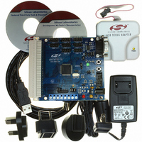
Evaluation Board, Power Supply, USB Cables, Adapter and Documentation
Processor To Be Evaluated
C8051F12x and C8051F13x
Interface Type
USB
Silicon Manufacturer
Silicon Labs
Core Architecture
8051
Silicon Core Number
C8051F120
Silicon Family Name
C8051F12x
Lead Free Status / RoHS Status
Contains lead / RoHS non-compliant
For Use With/related Products
C8051F120, 121, 122, 123, 124, 125, 126, 127
Lead Free Status / Rohs Status
Lead free / RoHS Compliant
Other names
336-1224
Available stocks
Company
Part Number
Manufacturer
Quantity
Price
Company:

Part Number:
C8051F120DK
Manufacturer:
SiliconL
Quantity:
4


1.9.
The C8051F12x devices have an on-board 8-bit SAR ADC (ADC2) with an 8-channel input multiplexer and
programmable gain amplifier. This ADC features a 500 ksps maximum throughput and true 8-bit linearity
with an INL of ±1LSB. Eight input pins are available for measurement. The ADC is under full control of the
CIP-51 microcontroller via the Special Function Registers. The ADC2 voltage reference is selected
between the analog power supply (AV+) and an external VREF pin. On the 100-pin TQFP devices, ADC2
has its own dedicated Voltage Reference input pin; on the 64-pin TQFP devices, ADC2 shares a Voltage
Reference input pin with ADC0. User software may put ADC2 into shutdown mode to save power.
A programmable gain amplifier follows the analog multiplexer. The gain stage can be especially useful
when different ADC input channels have widely varied input voltage signals, or when it is necessary to
"zoom in" on a signal with a large DC offset (in differential mode, a DAC could be used to provide the DC
offset). The PGA gain can be set in software to 0.5, 1, 2, or 4.
A flexible conversion scheduling system allows ADC2 conversions to be initiated by software commands,
timer overflows, or an external input signal. ADC2 conversions may also be synchronized with ADC0 soft-
ware-commanded conversions. Conversion completions are indicated by a status bit and an interrupt (if
enabled), and the resulting 8-bit data word is latched into an SFR upon completion.
AIN2.0
AIN2.1
AIN2.2
AIN2.3
AIN2.4
AIN2.5
AIN2.6
AIN2.7
8-Bit Analog to Digital Converter
Analog Multiplexer
AMUX
8-to-1
Figure 1.14. 8-Bit ADC Diagram
Programmable Gain
X
Amplifier
External VREF
Configuration, Control, and Data Registers
+
-
AV+
AV+
Pin
Rev. 1.4
C8051F120/1/2/3/4/5/6/7
ADC
VREF
8-Bit
SAR
Start Conversion
C8051F130/1/2/3
8
Compare
Window
Logic
Write to AD2BUSY
Timer 3 Overflow
CNVSTR2 Input
Timer 2 Overflow
Write to AD0BUSY
(synchronized with
ADC0)
ADC Data
Register
Conversion
Compare
Complete
Interrupt
Window
Interrupt
35
Related parts for C8051F120DK
Image
Part Number
Description
Manufacturer
Datasheet
Request
R

Part Number:
Description:
SMD/C°/SINGLE-ENDED OUTPUT SILICON OSCILLATOR
Manufacturer:
Silicon Laboratories Inc
Part Number:
Description:
Manufacturer:
Silicon Laboratories Inc
Datasheet:
Part Number:
Description:
N/A N/A/SI4010 AES KEYFOB DEMO WITH LCD RX
Manufacturer:
Silicon Laboratories Inc
Datasheet:
Part Number:
Description:
N/A N/A/SI4010 SIMPLIFIED KEY FOB DEMO WITH LED RX
Manufacturer:
Silicon Laboratories Inc
Datasheet:
Part Number:
Description:
N/A/-40 TO 85 OC/EZLINK MODULE; F930/4432 HIGH BAND (REV E/B1)
Manufacturer:
Silicon Laboratories Inc
Part Number:
Description:
EZLink Module; F930/4432 Low Band (rev e/B1)
Manufacturer:
Silicon Laboratories Inc
Part Number:
Description:
I°/4460 10 DBM RADIO TEST CARD 434 MHZ
Manufacturer:
Silicon Laboratories Inc
Part Number:
Description:
I°/4461 14 DBM RADIO TEST CARD 868 MHZ
Manufacturer:
Silicon Laboratories Inc
Part Number:
Description:
I°/4463 20 DBM RFSWITCH RADIO TEST CARD 460 MHZ
Manufacturer:
Silicon Laboratories Inc
Part Number:
Description:
I°/4463 20 DBM RADIO TEST CARD 868 MHZ
Manufacturer:
Silicon Laboratories Inc
Part Number:
Description:
I°/4463 27 DBM RADIO TEST CARD 868 MHZ
Manufacturer:
Silicon Laboratories Inc
Part Number:
Description:
I°/4463 SKYWORKS 30 DBM RADIO TEST CARD 915 MHZ
Manufacturer:
Silicon Laboratories Inc
Part Number:
Description:
N/A N/A/-40 TO 85 OC/4463 RFMD 30 DBM RADIO TEST CARD 915 MHZ
Manufacturer:
Silicon Laboratories Inc
Part Number:
Description:
I°/4463 20 DBM RADIO TEST CARD 169 MHZ
Manufacturer:
Silicon Laboratories Inc