DK-CYCII-2C20N Altera, DK-CYCII-2C20N Datasheet
DK-CYCII-2C20N
Specifications of DK-CYCII-2C20N
Available stocks


Related parts for DK-CYCII-2C20N


DK-CYCII-2C20N Summary of contents
Page 1
... Cyclone II FPGA Starter Development Kit 101 Innovation Drive San Jose, CA 95134 (408) 544-7000 http://www.altera.com P25-36048-00 User Guide Preliminary Information Document Version Document Date 1.0.0 October 2006 ...
Page 2
... Altera Corporation. Altera customers are advised to obtain the latest version of device specifications before relying on any published information and before placing orders for products or services Printed on recycled paper ii . UG-CDK01012-10 Altera Corporation ...
Page 3
... Read/Write Data .............................................................................................................................. 4–4 Sequential Write ............................................................................................................................... 4–5 Sequential Read ................................................................................................................................ 4–6 Flash Memory Programmer ................................................................................................................. 4–6 Read/Write Data .............................................................................................................................. 4–7 Sequential Write ............................................................................................................................... 4–8 Sequential Read ................................................................................................................................ 4–8 Configuring User Ports ......................................................................................................................... 4–9 Flash Music Player ................................................................................................................................. 4–9 VGA Display ........................................................................................................................................ 4–11 Displaying the Default Image ....................................................................................................... 4–11 Altera Corporation Contents iii ...
Page 4
... Chapter 6. Advanced Examples Factory Configuration ........................................................................................................................... 6–1 File Locations .................................................................................................................................... 6–1 Demonstration Setup ....................................................................................................................... 6–1 Music Synthesizer Demonstration ...................................................................................................... 6–2 File Locations .................................................................................................................................... 6–4 Demonstration Setup ....................................................................................................................... 6–4 SD Card Music Player ........................................................................................................................... 6–5 File Locations .................................................................................................................................... 6–6 Demonstration Setup ....................................................................................................................... 6–6 iv Cyclone II FPGA Starter Development Kit User Guide Altera Corporation ...
Page 5
... This user guide describes how to start using the Altera FPGA Starter Development Kit, including unpacking the kit, installing required software, connecting the development board to a PC, and running sample software. For a full description of the development board and its use, refer to the Cyclone II FPGA Starter Development Kit Reference Manual. ...
Page 6
... Typographic Conventions For the most up-to-date information about Altera products the Altera world-wide web site at www.altera.com. For technical support on this product www.altera.com/mysupport. For additional information about Altera products, consult the sources shown below. Information Type Technical support www.altera.com/mysupport/ (800) 800-EPLD (3753) (7:00 a ...
Page 7
... The warning indicates information that should be read prior to starting or w continuing the procedure or processes r The angled arrow indicates you should press the Enter key. f The feet direct you to more information on a particular topic. Altera Corporation October 2006 Meaning , Active-low signals are denoted by suffix input. c:\qdesigns\tutorial\chiptrip.gdf SUBDESIGN ), as well as logic function names (e ...
Page 8
... Typographic Conventions viii Cyclone II FPGA Starter Development Kit User Guide Altera Corporation October 2006 ...
Page 9
... October 2006 How to set up, power up, and verify correct operation of the development board How to install the Altera Development Suite Tools and the Cyclone II FPGA Starter Development Kit CD-ROMs How to set up, and use the Control Panel, a graphical user interface (GUI), to manipulate components on the board, implement ...
Page 10
... User Guide and Reference Manual, Control Panel utility, reference designs and demonstrations, device datasheets, tutorials, and a set of laboratory exercises The Altera Development Suite Tools CD-ROMs containing Altera ® Quartus II 6.0 Web Edition design software and the Nios ...
Page 11
... Figure 1–1. Board Stand Covers Software The instructions in this section describe how to install the following: Installation ■ ■ Altera Corporation October 2006 For Cyclone II Orcad symbols: http://www.altera.com/support/software/download/pcb/pcb- pcb_index.html For Nios II 32-bit embedded processor solutions: http://www.altera.com/technology/embedded/emb-index.html Before beginning any work, prepare the board as follows: ...
Page 12
... Programs > Altera > Cyclone II FPGA Starter Development Kit v1.0.0 icon, accessible from the Windows Start menu. Use this icon to launch the Windows-style development kit GUI. The Cyclone II FPGA Starter Development Kit installation program creates a directory structure for the installed files < ...
Page 13
... Table 1–1 Table 1–1. Installed Directory Contents BoardDesignFiles Docs Examples Installing the Quartus II Software Install the Quartus II Web Edition Software Suite found in the Altera Design Software Suite by performing the following steps The Quartus II software is the primary FPGA development tool used to create the reference designs used in this development kit. ...
Page 14
... Software Installation 1–6 Cyclone II FPGA Starter Development Kit User Guide Altera Corporation October 2006 ...
Page 15
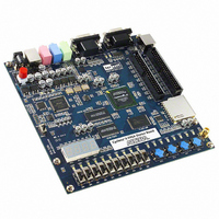
... Development Altera delivers the development board configuration to demonstrate features of the board. At power up, the Board Overview preloaded configuration also enables users to confirm quickly that the board is operating correctly. Figure 2–1. Cyclone II Development Board Layout and Components Requirements Preparation for using the development board requires the following ...
Page 16
... The Cyclone II FPGA Starter Development Board includes an integrated USB-Blaster™ chip set for programming the FPGA. Install the Altera USB-Blaster driver software on the host computer, if not already installed. Communication between the computer host and the development board requires Altera USB-Blaster driver software already installed on the host computer ...
Page 17
... Figure 2–2. Default VGA Output Pattern, SW0 = DOWN 4. Figure 2–3. Default FGA Output Pattern, SW0 = UP 5. Altera Corporation October 2006 Confirm that the VGA monitor displays the default image (Figure 2–3) with the SW0 switch set to the UP (away from the edge of the board) position ...
Page 18
... Confirm that the headset produces the expected music or recorded sounds playing on the audio player. If you also connect a microphone to the Mic In connector, the development board mixes the voice input with the output from the audio player. Altera Corporation October 2006 ...
Page 19
... Control Panel Setup “Using the Control Panel” Set up the hardware Configure the FPGA Start the Control Panel Install the Altera USB-Blaster driver software on the host computer, if not already installed ® Install the Altera Quartus software on the host computer, if not already installed “ ...
Page 20
... Next, click on the Program/Configure box to select the added file. Click Start to download the selected configuration file into the FPGA. Run the CII_Starter_control_panel.exe program found in the <kit path>\Examples\CII_Starter_demonstrations \CII_Starter_USB_API_v1\SW directory to launch the Control Panel user interface (Figure 3–2). Figure 3–1. Altera Corporation October 2006 ...
Page 21
... Figure 3–2. Control Panel Window Altera Corporation October 2006 Select Open to list all USB ports connected to development boards. The Control Panel can control development boards using the USB links. Select Open USB Port 0. This step places the Control Panel in control of the development board. ...
Page 22
... Control Panel Start 3–4 Cyclone II FPGA Starter Development Kit User Guide Altera Corporation October 2006 ...
Page 23
... Figure 4–1. Control Panel Access to the Development Board The user can perform the following actions with the Control Panel: ■ ■ ■ ■ Altera Corporation October 2006 4. Using the Control Panel Change the values that appear on the 7-segment displays Light up LEDs Communicate with the PS/2 keyboard ...
Page 24
... Load an image pattern for VGA output 3–2. Select the PS2 & LED tab on the Control Panel In the LED & 7-SEG area, enter a value for any of the 7-segment modules labeled HEX0 through HEX3. “Control Panel Start” on (Figure 4–2). Altera Corporation October 2006 ...
Page 25
... PS/2 interface commands and data. To test the functionality of the PS/2 keyboard interface, perform the following steps: 1. Altera Corporation October 2006 Click on the Set button. Select the PS2 & LED tab on the Control Panel In the LED & 7-SEG area, select the individual LEDs to turn on. ...
Page 26
... Read/write data from/to the SDRAM or SRAM on the development board Write sequential data or the entire contents of a file, to the SDRAM or SRAM Read sequential data or the entire contents of the SDRAM or SRAM to a file Select the SDRAM tab on the Control Panel (Figure 4–4). Altera Corporation October 2006 ...
Page 27
... To write the contents of a file into the SDRAM, use the Sequential Write function of the Control Panel to perform the following steps Altera Corporation October 2006 To write a 16-bit word into the SDRAM, use the Random Access boxes to enter the address of the desired location, specify the data to write, and click on the Write button. ...
Page 28
... Write one byte to the memory Read one byte from the memory Write a binary file to the memory Load the contents of the flash memory into a file When performing these operations, consider the following characteristics and limitations of the flash memory: Altera Corporation October 2006 ...
Page 29
... To perform a read/write operation with a byte of data from/to the flash memory, take the following steps: 1. Figure 4–5. Control Panel Flash Tab Window Altera Corporation October 2006 4 Mbits x 8 bits organization Erasure of the entire flash memory is required before writing into it Flash memory tolerates only a limited number of erasures Do not exit from the Control Panel while erasing the entire contents of the flash memory ...
Page 30
... Click on the Write a File to FLASH button to initiate the writing of the data. Specify the source file in the pop-up Windows dialog box. Select the FLASH tab on the Control Panel and use the Sequential Read boxes. Specify the starting address in the Address box. Altera Corporation October 2006 ...
Page 31
... To implement this application perform the following steps Altera Corporation October 2006 Specify the number of bytes of data to read from the flash memory in the Length box. To copy the entire contents of the flash memory into a file, only checkmark the Entire Flash box without specifying the number of bytes ...
Page 32
... Asynchronous 1 port of the Flash Controller. On the development board, set switches SW1 to OFF (DOWN position) and SW0 to ON (UP position). Plug a headset or a speaker into the audio output jack and listen to music produced through the Audio DAC circuit. Altera Corporation October 2006 ...
Page 33
... Displaying the Default Image Perform the following steps to display a default image: 1. Altera Corporation October 2006 Example 1 provides a default image previously loaded into an M4K memory block in the FPGA in the MIF/Hex (Intel) format during the default bit stream configuration stage (described in Cyclone II FPGA” ...
Page 34
... Control Panel displayed on the screen. Confirm that the cursor appears on the screen; manipulate it by moving the X/Y-axes scroll bars on the Control Panel. Select the SRAM tab of the Control Panel and load the file picture.dat into the SRAM. Altera Corporation October 2006 ...
Page 35
... Figure 4–8. Configuring the Port to Access the Image Data in the SRAM 3. Altera Corporation October 2006 Select the TOOLS tab and choose Asynchronous 1 for the SRAM Multiplexer port (Figure 4–8). Click on the Configure button to activate the multi-port setup in the FPGA (Figure 4–9). ...
Page 36
... Cyclone II FPGA Starter Development Kit User Guide Select the VGA tab and deselect the checkbox Default Image. Observe that the VGA monitor displays the picture.dat image from the SRAM (Figure 4–10). Turn off the cursor by deselecting the Cursor Enable checkbox. Altera Corporation October 2006 ...
Page 37
... FPGA, first generate a bitmap file. Perform the following steps Figure 4–11. The Image Converter Window 4. 5. Altera Corporation October 2006 Load the desired image into an image processing tool, such as ® ® Corel PhotoPaint . Resample the original image to have a 640 x 480 resolution. Save the modified image in the Windows bitmap format ...
Page 38
... Another Image from a Downloaded Bitmap File” on page 4–12. Table 4–1 defines the threshold for judging black or R/G/B Band Filter R/G/B R/G/B (optional) B&W Threshold Output Result Filter (640x480) N/A Raw_Data_Gray BW Threshold Raw_Data_BW + Raw_Data_BW.txt N/A Raw_Data_Gray BW Threshold Raw_Data_BW + Raw_Data_BW.txt Altera Corporation October 2006 ...
Page 39
... AS Programming In the Active Serial programming method, the configuration bit stream downloads into the Altera EPCS4 serial EEPROM chip. The EEPROM provides non-volatile storage of the bit stream, retaining the information even when power to the Cyclone II FPGA Starter board is turned off. When the board powers up, the configuration data in the EPCS4 device automatically loads into the Cyclone II FPGA ...
Page 40
... For both the JTAG and AS programming methods, the Cyclone II FPGA Starter board connects to a host computer via a USB cable. Because of this connection type, the host computer identifies the board as an Altera USB-Blaster device. The following sections describe the JTAG and AS programming steps. ...
Page 41
... Refer to the Serial Configuration Devices chapter in the Altera Configuration Device Handbook for more information about the EPCS4 device. Altera Corporation October 2006 illustrates the AS configuration setup. To download a Ensure that power is applied to the Cyclone II FPGA Starter board Connect the supplied USB cable to the USB-Blaster port on the ...
Page 42
... Configuring the Cyclone II FPGA Figure 5–2. The AS Configuration Scheme USB Blaster Circuit USB RUN/PROG MAX 3128 PROG” 5–4 Cyclone II FPGA Starter Development Kit User Guide Auto Power on Config EPCS Serial Configuration Device JTAG Config Port FPGA Altera Corporation October 2006 ...
Page 43
... Demonstration Setup To set up the demonstration, perform the following steps Altera Corporation October 2006 6. Advanced Examples Project directory: CII_Starter_Default Bit stream used: CII_Starter_Default.sof or CII_Starter_Default.pof Power up the development board with the USB cable connected to the USB-Blaster port. If necessary (that is, if the default factory ...
Page 44
... Place toggle switch SW9 in the UP position to hear a 1 kHz humming sound from the audio-out port. Alternatively, if switch SW9 is DOWN, connect the Mic In port to a microphone to hear voice sounds or use the line-in port to play audio from an appropriate sound source. Figure 6–1 shows the setup of the demonstration. Altera Corporation October 2006 ...
Page 45
... The TONE_GENERATOR can produce two tones, (1) String and (2) Brass, selected by SW0. The audio CODEC used on the development board has two channels, turned ON/OFF by SW1 and SW2. Figure 6–2. Block Diagram of the Music Synthesizer Design Altera Corporation October 2006 (Figure 6–2) shows that the Music Synthesizer DEMO_SOUND stores a sample sound for the user to play ...
Page 46
... Press KEY0 on the development board to reset the circuit. illustrates the usage of the switches and push buttons (KEYs). Signal Name KEY[0] Reset KEY[1] Repeat the Demo Music 0: BRASS T SW[0] SW[9] 0: DEMO play SW[1] 0: Channel-1 ON SW[2] 0: Channel-2 ON Description 1: STRING 1: PS2 KEYBOARD play 1: Channel-1 OFF 1: Channel-2 OFF Altera Corporation October 2006 ...
Page 47
... SD card and enables the board to play the music files via its CD-quality audio DAC circuits. The design uses the Nios II processor to read the music data stored in the SD Card and uses the Wolfson WM8731 audio CODEC to play the music. Altera Corporation October 2006 illustrates the usage of the PS/2 Keyboard. Signal Name ...
Page 48
... Demonstration Setup To set up the demonstration, perform the following steps: 6–6 Cyclone II FPGA Starter Development Kit User Guide 6–3) shows that the sample design provides an audio DAC Project directory: CII_Starter_SD_Card_Audio Bit stream used: CII_Starter_SD_Card_Audio.sof (or .pof) Nios II Workspace: CII_Starter_SD_Card_Audio Altera Corporation October 2006 ...
Page 49
... Figure 6–4 Figure 6–4. The Setup for the SD Music Player Demonstration Altera Corporation October 2006 Format the SD card into FAT16 format. Playing a music file with this demonstration requires that the file use the WAV format. Copy one or more such WAV files onto the FAT16-formatted SD card ...
Page 50
... SD Card Music Player 6–8 Cyclone II FPGA Starter Development Kit User Guide Altera Corporation October 2006 ...