C8051F330DK Silicon Laboratories Inc, C8051F330DK Datasheet - Page 24
C8051F330DK
Manufacturer Part Number
C8051F330DK
Description
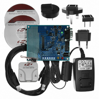
DEV KIT FOR C8051F330/F331
Manufacturer
Silicon Laboratories Inc
Type
MCUr
Specifications of C8051F330DK
Contents
Evaluation Board, Power Supply, USB Cables, Adapter and Documentation
Processor To Be Evaluated
C8051F33x
Interface Type
RS-232
Operating Supply Voltage
7 V to 15 V
Silicon Manufacturer
Silicon Labs
Core Architecture
8051
Silicon Core Number
C8051F330
Silicon Family Name
C8051F33x
Lead Free Status / RoHS Status
Contains lead / RoHS non-compliant
For Use With/related Products
Silicon Laboratories C8051F330, C8051F331
Lead Free Status / Rohs Status
Lead free / RoHS Compliant
Other names
336-1264


C8051F330/1/2/3/4/5
1.4.
C8051F330/1/2/3/4/5 devices include 17 I/O pins (two byte-wide Ports and one 1-bit-wide Port). The
C8051F330/1/2/3/4/5 Ports behave like typical 8051 Ports with a few enhancements. Each Port pin may be
configured as an analog input or a digital I/O pin. Pins selected as digital I/Os may additionally be config-
ured for push-pull or open-drain output. The “weak pullups” that are fixed on typical 8051 devices may be
globally disabled, providing power savings capabilities.
The Digital Crossbar allows mapping of internal digital system resources to Port I/O pins. (See
Figure 1.11.) On-chip counter/timers, serial buses, HW interrupts, comparator output, and other digital sig-
nals in the controller can be configured to appear on the Port I/O pins specified in the Crossbar Control
registers. This allows the user to select the exact mix of general purpose Port I/O and digital resources
needed for the particular application.
1.5.
The C8051F330/1/2/3/4/5 Family includes an SMBus/I
baud rate configuration, and an Enhanced SPI interface. Each of the serial buses is fully implemented in
hardware and makes extensive use of the CIP-51's interrupts, thus requiring very little CPU intervention.
26
Highest
Priority
Lowest
Priority
Programmable Digital I/O and Crossbar
Serial Ports
SYSCLK
Outputs
SMBus
T0, T1
UART
P0
P1
CP0
PCA
SPI
(P0.0-P0.7)
(P1.0-P1.7)
Figure 1.11. Digital Crossbar Diagram
2
4
2
2
4
2
8
8
Rev. 1.7
PnSKIP Registers
XBR0, XBR1,
Crossbar
Decoder
Priority
Digital
2
C interface, a full-duplex UART with enhanced
8
8
PnMDIN Registers
PnMDOUT,
Cells
Cells
I/O
I/O
P0
P1
P0.0
P0.7
P1.0
P1.7
Related parts for C8051F330DK
Image
Part Number
Description
Manufacturer
Datasheet
Request
R

Part Number:
Description:
SMD/C°/SINGLE-ENDED OUTPUT SILICON OSCILLATOR
Manufacturer:
Silicon Laboratories Inc
Part Number:
Description:
Manufacturer:
Silicon Laboratories Inc
Datasheet:
Part Number:
Description:
N/A N/A/SI4010 AES KEYFOB DEMO WITH LCD RX
Manufacturer:
Silicon Laboratories Inc
Datasheet:
Part Number:
Description:
N/A N/A/SI4010 SIMPLIFIED KEY FOB DEMO WITH LED RX
Manufacturer:
Silicon Laboratories Inc
Datasheet:
Part Number:
Description:
N/A/-40 TO 85 OC/EZLINK MODULE; F930/4432 HIGH BAND (REV E/B1)
Manufacturer:
Silicon Laboratories Inc
Part Number:
Description:
EZLink Module; F930/4432 Low Band (rev e/B1)
Manufacturer:
Silicon Laboratories Inc
Part Number:
Description:
I°/4460 10 DBM RADIO TEST CARD 434 MHZ
Manufacturer:
Silicon Laboratories Inc
Part Number:
Description:
I°/4461 14 DBM RADIO TEST CARD 868 MHZ
Manufacturer:
Silicon Laboratories Inc
Part Number:
Description:
I°/4463 20 DBM RFSWITCH RADIO TEST CARD 460 MHZ
Manufacturer:
Silicon Laboratories Inc
Part Number:
Description:
I°/4463 20 DBM RADIO TEST CARD 868 MHZ
Manufacturer:
Silicon Laboratories Inc
Part Number:
Description:
I°/4463 27 DBM RADIO TEST CARD 868 MHZ
Manufacturer:
Silicon Laboratories Inc
Part Number:
Description:
I°/4463 SKYWORKS 30 DBM RADIO TEST CARD 915 MHZ
Manufacturer:
Silicon Laboratories Inc
Part Number:
Description:
N/A N/A/-40 TO 85 OC/4463 RFMD 30 DBM RADIO TEST CARD 915 MHZ
Manufacturer:
Silicon Laboratories Inc
Part Number:
Description:
I°/4463 20 DBM RADIO TEST CARD 169 MHZ
Manufacturer:
Silicon Laboratories Inc