C8051F330DK Silicon Laboratories Inc, C8051F330DK Datasheet - Page 41
C8051F330DK
Manufacturer Part Number
C8051F330DK
Description
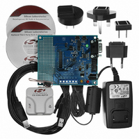
DEV KIT FOR C8051F330/F331
Manufacturer
Silicon Laboratories Inc
Type
MCUr
Specifications of C8051F330DK
Contents
Evaluation Board, Power Supply, USB Cables, Adapter and Documentation
Processor To Be Evaluated
C8051F33x
Interface Type
RS-232
Operating Supply Voltage
7 V to 15 V
Silicon Manufacturer
Silicon Labs
Core Architecture
8051
Silicon Core Number
C8051F330
Silicon Family Name
C8051F33x
Lead Free Status / RoHS Status
Contains lead / RoHS non-compliant
For Use With/related Products
Silicon Laboratories C8051F330, C8051F331
Lead Free Status / Rohs Status
Lead free / RoHS Compliant
Other names
336-1264


C8051F330/1/2/3/4/5
5.3.1. Starting a Conversion
A conversion can be initiated in one of six ways, depending on the programmed states of the ADC0 Start of
Conversion Mode bits (AD0CM2–0) in register ADC0CN. Conversions may be initiated by one of the fol-
lowing:
Writing a ‘1’ to AD0BUSY provides software control of ADC0 whereby conversions are performed "on-
demand". During conversion, the AD0BUSY bit is set to logic 1 and reset to logic 0 when the conversion is
complete. The falling edge of AD0BUSY triggers an interrupt (when enabled) and sets the ADC0 interrupt
flag (AD0INT). Note: When polling for ADC conversion completions, the ADC0 interrupt flag (AD0INT)
should be used. Converted data is available in the ADC0 data registers, ADC0H:ADC0L, when bit AD0INT
is logic 1. Note that when Timer 2 or Timer 3 overflows are used as the conversion source, Low Byte over-
flows are used if Timer 2/3 is in 8-bit mode; High byte overflows are used if Timer 2/3 is in 16-bit mode.
See
Important Note About Using CNVSTR: The CNVSTR input pin also functions as Port pin P0.6. When the
CNVSTR input is used as the ADC0 conversion source, Port pin P0.6 should be skipped by the Digital
Crossbar. To configure the Crossbar to skip P0.6, set to ‘1’ Bit6 in register P0SKIP. See
Input/Output” on page 123
44
Section “18. Timers” on page 177
1. Writing a ‘1’ to the AD0BUSY bit of register ADC0CN
2. A Timer 0 overflow (i.e., timed continuous conversions)
3. A Timer 2 overflow
4. A Timer 1 overflow
5. A rising edge on the CNVSTR input signal (pin P0.6)
6. A Timer 3 overflow
for details on Port I/O configuration.
for timer configuration.
Rev. 1.7
Section “14. Port
Related parts for C8051F330DK
Image
Part Number
Description
Manufacturer
Datasheet
Request
R

Part Number:
Description:
SMD/C°/SINGLE-ENDED OUTPUT SILICON OSCILLATOR
Manufacturer:
Silicon Laboratories Inc
Part Number:
Description:
Manufacturer:
Silicon Laboratories Inc
Datasheet:
Part Number:
Description:
N/A N/A/SI4010 AES KEYFOB DEMO WITH LCD RX
Manufacturer:
Silicon Laboratories Inc
Datasheet:
Part Number:
Description:
N/A N/A/SI4010 SIMPLIFIED KEY FOB DEMO WITH LED RX
Manufacturer:
Silicon Laboratories Inc
Datasheet:
Part Number:
Description:
N/A/-40 TO 85 OC/EZLINK MODULE; F930/4432 HIGH BAND (REV E/B1)
Manufacturer:
Silicon Laboratories Inc
Part Number:
Description:
EZLink Module; F930/4432 Low Band (rev e/B1)
Manufacturer:
Silicon Laboratories Inc
Part Number:
Description:
I°/4460 10 DBM RADIO TEST CARD 434 MHZ
Manufacturer:
Silicon Laboratories Inc
Part Number:
Description:
I°/4461 14 DBM RADIO TEST CARD 868 MHZ
Manufacturer:
Silicon Laboratories Inc
Part Number:
Description:
I°/4463 20 DBM RFSWITCH RADIO TEST CARD 460 MHZ
Manufacturer:
Silicon Laboratories Inc
Part Number:
Description:
I°/4463 20 DBM RADIO TEST CARD 868 MHZ
Manufacturer:
Silicon Laboratories Inc
Part Number:
Description:
I°/4463 27 DBM RADIO TEST CARD 868 MHZ
Manufacturer:
Silicon Laboratories Inc
Part Number:
Description:
I°/4463 SKYWORKS 30 DBM RADIO TEST CARD 915 MHZ
Manufacturer:
Silicon Laboratories Inc
Part Number:
Description:
N/A N/A/-40 TO 85 OC/4463 RFMD 30 DBM RADIO TEST CARD 915 MHZ
Manufacturer:
Silicon Laboratories Inc
Part Number:
Description:
I°/4463 20 DBM RADIO TEST CARD 169 MHZ
Manufacturer:
Silicon Laboratories Inc