C8051F330DK Silicon Laboratories Inc, C8051F330DK Datasheet - Page 54
C8051F330DK
Manufacturer Part Number
C8051F330DK
Description
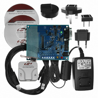
DEV KIT FOR C8051F330/F331
Manufacturer
Silicon Laboratories Inc
Type
MCUr
Specifications of C8051F330DK
Contents
Evaluation Board, Power Supply, USB Cables, Adapter and Documentation
Processor To Be Evaluated
C8051F33x
Interface Type
RS-232
Operating Supply Voltage
7 V to 15 V
Silicon Manufacturer
Silicon Labs
Core Architecture
8051
Silicon Core Number
C8051F330
Silicon Family Name
C8051F33x
Lead Free Status / RoHS Status
Contains lead / RoHS non-compliant
For Use With/related Products
Silicon Laboratories C8051F330, C8051F331
Lead Free Status / Rohs Status
Lead free / RoHS Compliant
Other names
336-1264


6. 10-Bit Current Mode DAC (IDA0, C8051F330 only)
The C8051F330 device includes a 10-bit current-mode Digital-to-Analog Converter (IDAC). The maximum
current output of the IDAC can be adjusted for three different current settings; 0.5 mA, 1 mA, and 2 mA.
The IDAC is enabled or disabled with the IDA0EN bit in the IDA0 Control Register (see SFR Definition 6.1).
When IDA0EN is set to ‘0’, the IDAC port pin (P0.1) behaves as a normal GPIO pin. When IDA0EN is set
to ‘1’, the digital output drivers and weak pullup for the IDAC pin are automatically disabled, and the pin is
connected to the IDAC output. An internal bandgap bias generator is used to generate a reference current
for the IDAC whenever it is enabled. When using the IDAC, bit 1 in the P0SKIP register should be set to ‘1’,
to force the Crossbar to skip the IDAC pin.
6.1.
IDA0 features a flexible output update mechanism which allows for seamless full-scale changes and sup-
ports jitter-free updates for waveform generation. Three update modes are provided, allowing IDAC output
updates on a write to IDA0H, on a Timer overflow, or on an external pin edge.
6.1.1. Update Output On-Demand
In its default mode (IDA0CN.[6:4] = ‘111’) the IDA0 output is updated “on-demand” on a write to the high-
byte of the IDA0 data register (IDA0H). It is important to note that writes to IDA0L are held in this mode,
and have no effect on the IDA0 output until a write to IDA0H takes place. If writing a full 10-bit word to the
IDAC data registers, the 10-bit data word is written to the low byte (IDA0L) and high byte (IDA0H) data reg-
isters. Data is latched into IDA0 after a write to the IDA0H register, so the write sequence should be
IDA0L followed by IDA0H if the full 10-bit resolution is required. The IDAC can be used in 8-bit mode by
initializing IDA0L to the desired value (typically 0x00), and writing data to only IDA0H (see
information on the format of the 10-bit IDAC data word within the 16-bit SFR space).
IDA0 Output Scheduling
IDA0OMD1
IDA0OMD0
IDA0CM2
IDA0CM1
IDA0CM0
IDA0EN
Figure 6.1. IDA0 Functional Block Diagram
8
2
10
Rev. 1.7
IDA0
C8051F330/1/2/3/4/5
Section 6.2
IDA0
for
57
Related parts for C8051F330DK
Image
Part Number
Description
Manufacturer
Datasheet
Request
R

Part Number:
Description:
SMD/C°/SINGLE-ENDED OUTPUT SILICON OSCILLATOR
Manufacturer:
Silicon Laboratories Inc
Part Number:
Description:
Manufacturer:
Silicon Laboratories Inc
Datasheet:
Part Number:
Description:
N/A N/A/SI4010 AES KEYFOB DEMO WITH LCD RX
Manufacturer:
Silicon Laboratories Inc
Datasheet:
Part Number:
Description:
N/A N/A/SI4010 SIMPLIFIED KEY FOB DEMO WITH LED RX
Manufacturer:
Silicon Laboratories Inc
Datasheet:
Part Number:
Description:
N/A/-40 TO 85 OC/EZLINK MODULE; F930/4432 HIGH BAND (REV E/B1)
Manufacturer:
Silicon Laboratories Inc
Part Number:
Description:
EZLink Module; F930/4432 Low Band (rev e/B1)
Manufacturer:
Silicon Laboratories Inc
Part Number:
Description:
I°/4460 10 DBM RADIO TEST CARD 434 MHZ
Manufacturer:
Silicon Laboratories Inc
Part Number:
Description:
I°/4461 14 DBM RADIO TEST CARD 868 MHZ
Manufacturer:
Silicon Laboratories Inc
Part Number:
Description:
I°/4463 20 DBM RFSWITCH RADIO TEST CARD 460 MHZ
Manufacturer:
Silicon Laboratories Inc
Part Number:
Description:
I°/4463 20 DBM RADIO TEST CARD 868 MHZ
Manufacturer:
Silicon Laboratories Inc
Part Number:
Description:
I°/4463 27 DBM RADIO TEST CARD 868 MHZ
Manufacturer:
Silicon Laboratories Inc
Part Number:
Description:
I°/4463 SKYWORKS 30 DBM RADIO TEST CARD 915 MHZ
Manufacturer:
Silicon Laboratories Inc
Part Number:
Description:
N/A N/A/-40 TO 85 OC/4463 RFMD 30 DBM RADIO TEST CARD 915 MHZ
Manufacturer:
Silicon Laboratories Inc
Part Number:
Description:
I°/4463 20 DBM RADIO TEST CARD 169 MHZ
Manufacturer:
Silicon Laboratories Inc