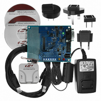
C8051F330DK Silicon Laboratories Inc, C8051F330DK Datasheet - Page 55

C8051F330DK
Manufacturer Part Number
C8051F330DK
Description
DEV KIT FOR C8051F330/F331
Manufacturer
Silicon Laboratories Inc
Type
MCUr
Specifications of C8051F330DK
Contents
Evaluation Board, Power Supply, USB Cables, Adapter and Documentation
Processor To Be Evaluated
C8051F33x
Interface Type
RS-232
Operating Supply Voltage
7 V to 15 V
Silicon Manufacturer
Silicon Labs
Core Architecture
8051
Silicon Core Number
C8051F330
Silicon Family Name
C8051F33x
Lead Free Status / RoHS Status
Contains lead / RoHS non-compliant
For Use With/related Products
Silicon Laboratories C8051F330, C8051F331
Lead Free Status / Rohs Status
Lead free / RoHS Compliant
Other names
336-1264
- Current page: 55 of 210
- Download datasheet (2Mb)
C8051F330/1/2/3/4/5
6.1.2. Update Output Based on Timer Overflow
Similar to the ADC operation, in which an ADC conversion can be initiated by a timer overflow indepen-
dently of the processor, the IDAC outputs can use a Timer overflow to schedule an output update event.
This feature is useful in systems where the IDAC is used to generate a waveform of a defined sampling
rate by eliminating the effects of variable interrupt latency and instruction execution on the timing of the
IDAC output. When the IDA0CM bits (IDA0CN.[6:4]) are set to ‘000’, ‘001’, ‘010’ or ‘011’, writes to both
IDAC data registers (IDA0L and IDA0H) are held until an associated Timer overflow event (Timer 0,
Timer 1, Timer 2 or Timer 3, respectively) occurs, at which time the IDA0H:IDA0L contents are copied to
the IDAC input latches, allowing the IDAC output to change to the new value.
6.1.3. Update Output Based on CNVSTR Edge
The IDAC output can also be configured to update on a rising edge, falling edge, or both edges of the
external CNVSTR signal. When the IDA0CM bits (IDA0CN.[6:4]) are set to ‘100’, ‘101’, or ‘110’, writes to
both IDAC data registers (IDA0L and IDA0H) are held until an edge occurs on the CNVSTR input pin. The
particular setting of the IDA0CM bits determines whether IDAC outputs are updated on rising, falling, or
both edges of CNVSTR. When a corresponding edge occurs, the IDA0H:IDA0L contents are copied to the
IDAC input latches, allowing the IDAC output to change to the new value.
6.2.
The IDAC data registers (IDA0H and IDA0L) are left-justified, meaning that the eight MSBs of the IDAC
output word are mapped to bits 7–0 of the IDA0H register, and the two LSBs of the IDAC output word are
mapped to bits 7 and 6 of the IDA0L register. The data word mapping for the IDAC is shown in Figure 6.2.
The full-scale output current of the IDAC is selected using the IDA0OMD bits (IDA0CN[1:0]). By default,
the IDAC is set to a full-scale output current of 2 mA. The IDA0OMD bits can also be configured to provide
full-scale output currents of 1 mA or 0.5 mA, as shown in SFR Definition 6.1.
58
Input Data Word
D9
IDAC Output Mapping
(D9–D0)
0x3FF
0x000
0x001
0x200
D8
D7
D6
IDA0H
IDA0OMD[1:0] = ‘1x’
1023/1024 x 2 mA
512/1024 x 2 mA
Output Current
1/1024 x 2 mA
Figure 6.2. IDA0 Data Word Mapping
D5
0 mA
D4
D3
D2
Rev. 1.7
IDA0OMD[1:0] = ‘01’
1023/1024 x 1 mA
512/1024 x 1 mA
Output Current
D1
1/1024 x 1 mA
0 mA
D0
IDA0L
IDA0OMD[1:0] = ‘00’
1023/1024 x 0.5 mA
512/1024 x 0.5 mA
1/1024 x 0.5 mA
Output Current
0 mA
Related parts for C8051F330DK
Image
Part Number
Description
Manufacturer
Datasheet
Request
R
Part Number:
Description:
SMD/C°/SINGLE-ENDED OUTPUT SILICON OSCILLATOR
Manufacturer:
Silicon Laboratories Inc
Part Number:
Description:
Manufacturer:
Silicon Laboratories Inc
Datasheet:
Part Number:
Description:
N/A N/A/SI4010 AES KEYFOB DEMO WITH LCD RX
Manufacturer:
Silicon Laboratories Inc
Datasheet:
Part Number:
Description:
N/A N/A/SI4010 SIMPLIFIED KEY FOB DEMO WITH LED RX
Manufacturer:
Silicon Laboratories Inc
Datasheet:
Part Number:
Description:
N/A/-40 TO 85 OC/EZLINK MODULE; F930/4432 HIGH BAND (REV E/B1)
Manufacturer:
Silicon Laboratories Inc
Part Number:
Description:
EZLink Module; F930/4432 Low Band (rev e/B1)
Manufacturer:
Silicon Laboratories Inc
Part Number:
Description:
I°/4460 10 DBM RADIO TEST CARD 434 MHZ
Manufacturer:
Silicon Laboratories Inc
Part Number:
Description:
I°/4461 14 DBM RADIO TEST CARD 868 MHZ
Manufacturer:
Silicon Laboratories Inc
Part Number:
Description:
I°/4463 20 DBM RFSWITCH RADIO TEST CARD 460 MHZ
Manufacturer:
Silicon Laboratories Inc
Part Number:
Description:
I°/4463 20 DBM RADIO TEST CARD 868 MHZ
Manufacturer:
Silicon Laboratories Inc
Part Number:
Description:
I°/4463 27 DBM RADIO TEST CARD 868 MHZ
Manufacturer:
Silicon Laboratories Inc
Part Number:
Description:
I°/4463 SKYWORKS 30 DBM RADIO TEST CARD 915 MHZ
Manufacturer:
Silicon Laboratories Inc
Part Number:
Description:
N/A N/A/-40 TO 85 OC/4463 RFMD 30 DBM RADIO TEST CARD 915 MHZ
Manufacturer:
Silicon Laboratories Inc
Part Number:
Description:
I°/4463 20 DBM RADIO TEST CARD 169 MHZ
Manufacturer:
Silicon Laboratories Inc


