C8051F330DK Silicon Laboratories Inc, C8051F330DK Datasheet - Page 7
C8051F330DK
Manufacturer Part Number
C8051F330DK
Description
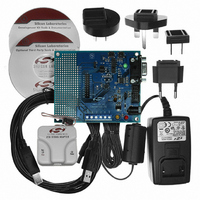
DEV KIT FOR C8051F330/F331
Manufacturer
Silicon Laboratories Inc
Type
MCUr
Specifications of C8051F330DK
Contents
Evaluation Board, Power Supply, USB Cables, Adapter and Documentation
Processor To Be Evaluated
C8051F33x
Interface Type
RS-232
Operating Supply Voltage
7 V to 15 V
Silicon Manufacturer
Silicon Labs
Core Architecture
8051
Silicon Core Number
C8051F330
Silicon Family Name
C8051F33x
Lead Free Status / RoHS Status
Contains lead / RoHS non-compliant
For Use With/related Products
Silicon Laboratories C8051F330, C8051F331
Lead Free Status / Rohs Status
Lead free / RoHS Compliant
Other names
336-1264


List of Figures
1. System Overview
2. Absolute Maximum Ratings
3. Global Electrical Characteristics
4. Pinout and Package Definitions
5. 10-Bit ADC (ADC0, C8051F330/2/4 only)
6. 10-Bit Current Mode DAC (IDA0, C8051F330 only)
7. Voltage Reference (C8051F330/2/4 only)
8. Comparator0
9. CIP-51 Microcontroller
10. Reset Sources
Figure 1.1. C8051F330 Block Diagram.................................................................... 19
Figure 1.2. C8051F331 Block Diagram.................................................................... 19
Figure 1.3. C8051F332 Block Diagram.................................................................... 20
Figure 1.4. C8051F333 Block Diagram.................................................................... 20
Figure 1.5. C8051F334 Block Diagram.................................................................... 21
Figure 1.6. C8051F335 Block Diagram.................................................................... 21
Figure 1.7. Comparison of Peak MCU Execution Speeds ....................................... 22
Figure 1.8. On-Chip Clock and Reset ...................................................................... 23
Figure 1.9. On-Board Memory Map ......................................................................... 24
Figure 1.10. Development/In-System Debug Diagram............................................. 25
Figure 1.11. Digital Crossbar Diagram ..................................................................... 26
Figure 1.12. PCA Block Diagram.............................................................................. 27
Figure 1.13. PCA Block Diagram.............................................................................. 27
Figure 1.14. 10-Bit ADC Block Diagram ................................................................... 28
Figure 1.15. Comparator0 Block Diagram ................................................................ 29
Figure 1.16. IDA0 Functional Block Diagram ........................................................... 30
Figure 4.1. QFN-20 Pinout Diagram (Top View)...................................................... 37
Figure 5.1. ADC0 Functional Block Diagram ........................................................... 41
Figure 5.2. Typical Temperature Sensor Transfer Function .................................... 43
Figure 5.3. 10-Bit ADC Track and Conversion Example Timing.............................. 45
Figure 5.4. ADC0 Equivalent Input Circuits ............................................................. 46
Figure 5.5. ADC Window Compare Example: Right-Justified Single-Ended Data... 53
Figure 5.6. ADC Window Compare Example: Left-Justified Single-Ended Data ..... 53
Figure 5.7. ADC Window Compare Example: Right-Justified Differential Data ....... 54
Figure 5.8. ADC Window Compare Example: Left-Justified Differential Data ......... 54
Figure 6.1. IDA0 Functional Block Diagram............................................................. 57
Figure 6.2. IDA0 Data Word Mapping...................................................................... 58
Figure 7.1. Voltage Reference Functional Block Diagram ....................................... 61
Figure 8.1. Comparator0 Functional Block Diagram................................................ 65
Figure 8.2. Comparator Hysteresis Plot................................................................... 66
Figure 9.1. CIP-51 Block Diagram ........................................................................... 71
Figure 9.2. Memory Map.......................................................................................... 77
Figure 10.1. Reset Sources...................................................................................... 97
Rev. 1.7
C8051F330/1/2/3/4/5
7
Related parts for C8051F330DK
Image
Part Number
Description
Manufacturer
Datasheet
Request
R

Part Number:
Description:
SMD/C°/SINGLE-ENDED OUTPUT SILICON OSCILLATOR
Manufacturer:
Silicon Laboratories Inc
Part Number:
Description:
Manufacturer:
Silicon Laboratories Inc
Datasheet:
Part Number:
Description:
N/A N/A/SI4010 AES KEYFOB DEMO WITH LCD RX
Manufacturer:
Silicon Laboratories Inc
Datasheet:
Part Number:
Description:
N/A N/A/SI4010 SIMPLIFIED KEY FOB DEMO WITH LED RX
Manufacturer:
Silicon Laboratories Inc
Datasheet:
Part Number:
Description:
N/A/-40 TO 85 OC/EZLINK MODULE; F930/4432 HIGH BAND (REV E/B1)
Manufacturer:
Silicon Laboratories Inc
Part Number:
Description:
EZLink Module; F930/4432 Low Band (rev e/B1)
Manufacturer:
Silicon Laboratories Inc
Part Number:
Description:
I°/4460 10 DBM RADIO TEST CARD 434 MHZ
Manufacturer:
Silicon Laboratories Inc
Part Number:
Description:
I°/4461 14 DBM RADIO TEST CARD 868 MHZ
Manufacturer:
Silicon Laboratories Inc
Part Number:
Description:
I°/4463 20 DBM RFSWITCH RADIO TEST CARD 460 MHZ
Manufacturer:
Silicon Laboratories Inc
Part Number:
Description:
I°/4463 20 DBM RADIO TEST CARD 868 MHZ
Manufacturer:
Silicon Laboratories Inc
Part Number:
Description:
I°/4463 27 DBM RADIO TEST CARD 868 MHZ
Manufacturer:
Silicon Laboratories Inc
Part Number:
Description:
I°/4463 SKYWORKS 30 DBM RADIO TEST CARD 915 MHZ
Manufacturer:
Silicon Laboratories Inc
Part Number:
Description:
N/A N/A/-40 TO 85 OC/4463 RFMD 30 DBM RADIO TEST CARD 915 MHZ
Manufacturer:
Silicon Laboratories Inc
Part Number:
Description:
I°/4463 20 DBM RADIO TEST CARD 169 MHZ
Manufacturer:
Silicon Laboratories Inc